Semiconductor memory device that requires refresh operations

a memory device and memory technology, applied in the field of semiconductor memory devices, can solve problems such as degenerate bits provided in rom circuits

Inactive Publication Date: 2007-05-08
LONGITUDE LICENSING LTD
View PDF4 Cites 13 Cited by
  • Summary
  • Abstract
  • Description
  • Claims
  • Application Information

AI Technical Summary

Benefits of technology

[0010]It is an object of the present invention to provide a semiconductor memory device that can save a refresh defective cell while effectively restricting variation in the power supply potential and the ground potential.
[0014]According to the present invention, because the appearance pattern of the multiple refresh is limited, a pattern having a risk of a large variation in the power supply potential or the ground potential such as a pattern of continuous occurrence of the multiple refresh can be excluded. Accordingly, the refresh defective cell can be relieved while restricting a variation in the power supply potential or the ground potential.

Problems solved by technology

However, when the actual product design is considered, in some cases, a degenerate bit is provided in the ROM circuit due to a constraint of trade off between the mounting area of the ROM circuit and productivity.

Method used


Image

  • Semiconductor memory device that requires refresh operations
  • Semiconductor memory device that requires refresh operations
  • Semiconductor memory device that requires refresh operations

Examples


Embodiment Construction

[0029]Preferred embodiments of the present invention will now be explained in detail with reference to the drawings.

[0030]FIG. 1 is a block diagram showing a configuration of a semiconductor memory device 100 according to a preferred embodiment of the present invention.

[0031]As shown in FIG. 1, the semiconductor memory device 100 according to the present embodiment includes memory arrays 101 to 104. The semiconductor memory device 100 has a read function of reading data stored in an address supplied via an address pin ADD, and outputting the stored data via a data pin DQ. The semiconductor memory device 100 also has a write function of writing the data supplied via the data pin DQ into the address supplied via the address pin ADD. While the four memory arrays are provided in this embodiment as an example, the number of memory arrays is not particularly limited in the present invention, and one memory array can be divided into plural sub-arrays.

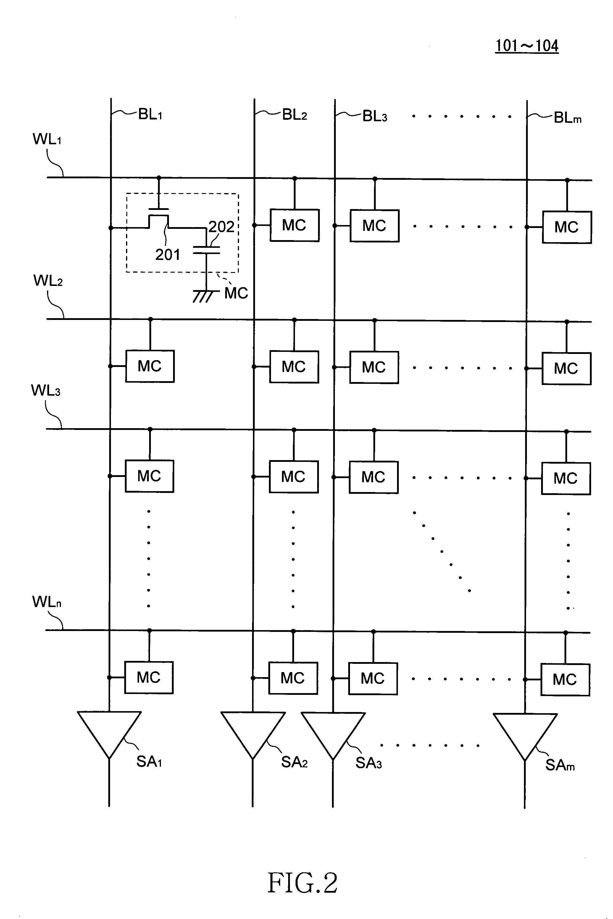
[0032]FIG. 2 is a circuit diagram showi...


PUM


Abstract

A semiconductor memory device includes a refresh counter that outputs an address of a word line to be refreshed, a ROM circuit that stores a relevant address related to a refresh defective address, and a multiple refresh control circuit that simultaneously or continuously activates the refresh defective address and the relevant address within one refresh cycle in response to a fact that the ROM circuit detects the relevant address. The multiple refresh control circuit excludes a pattern having a risk that a power supply potential or a ground potential varies greatly such as a pattern that the multiple refresh occurs continuously. With this arrangement, a refresh defective cell can be saved while restricting the variation in the power supply potential or the ground potential.

Description

TECHNICAL FIELD[0001]The present invention relates to a semiconductor memory device. Particularly, the present invention relates to a semiconductor memory device that requires refresh operations such as a DRAM (Dynamic Random Access Memory).BACKGROUND OF THE INVENTION[0002]The density of a DRAM can be most suitably increased among various kinds of semiconductor memory devices, and the DRAM is widely used for a main memory of a computer and the like. The prime reason that the density of the DRAM can be most suitably increased is that the structure of the memory cell of the DRAM is remarkably simple as compared with that of other semiconductor memory devices. In other words, the memory cell of the DRAM consists of one capacitor and one MOS transistor, and stores information based on a charge stored in the capacitor. Charging to and discharging from the capacitor is controlled by a MOS transistor whose gate electrode is connected to a word line. When the MOS transistor is turned on, a ...

Claims


Application Information

Patent Timeline
Patent Type & Authority Patents(United States)
IPC IPC(8): G11C7/00G11C8/00
CPCG11C11/406G11C11/40622G11C29/783
Inventor DONO, CHIAKIKOSHIKAWA, YASUJI
Owner LONGITUDE LICENSING LTD
Why Eureka
Try Eureka