

Photoelectric conversion film-stacked type solid-state imaging device
a technology of photoelectric conversion and solid-state imaging, which is applied in the direction of semiconductor devices, radiation controlled devices, picture signal generators, etc., can solve the problems of reducing light utilization efficiency, reducing sensitivity, and reducing the total area of the photo acceptance portion, so as to reduce the manufacturing cost
- Summary
- Abstract
- Description
- Claims
- Application Information
AI Technical Summary
Benefits of technology
Problems solved by technology
Method used
Image

Examples
first embodiment
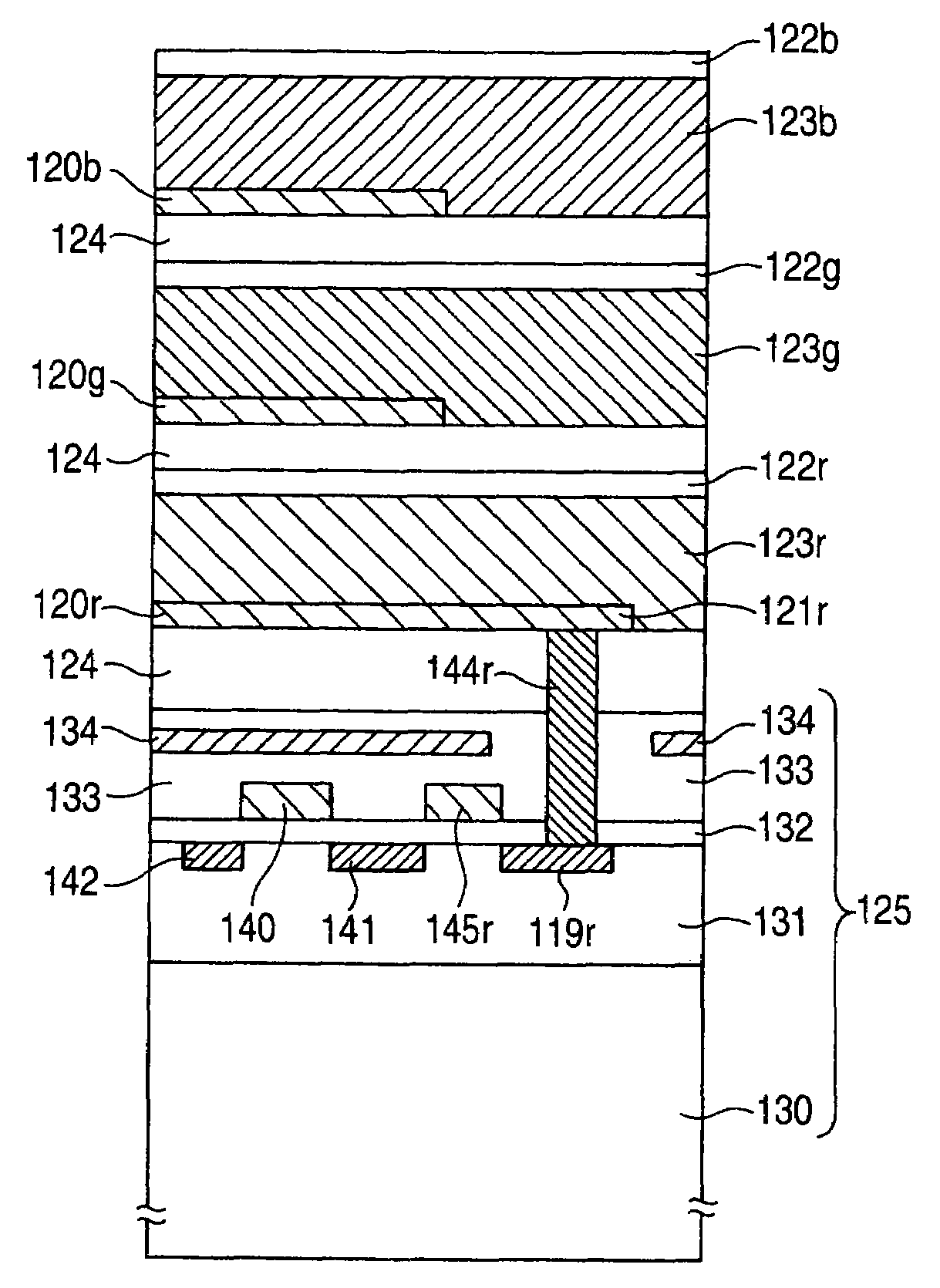
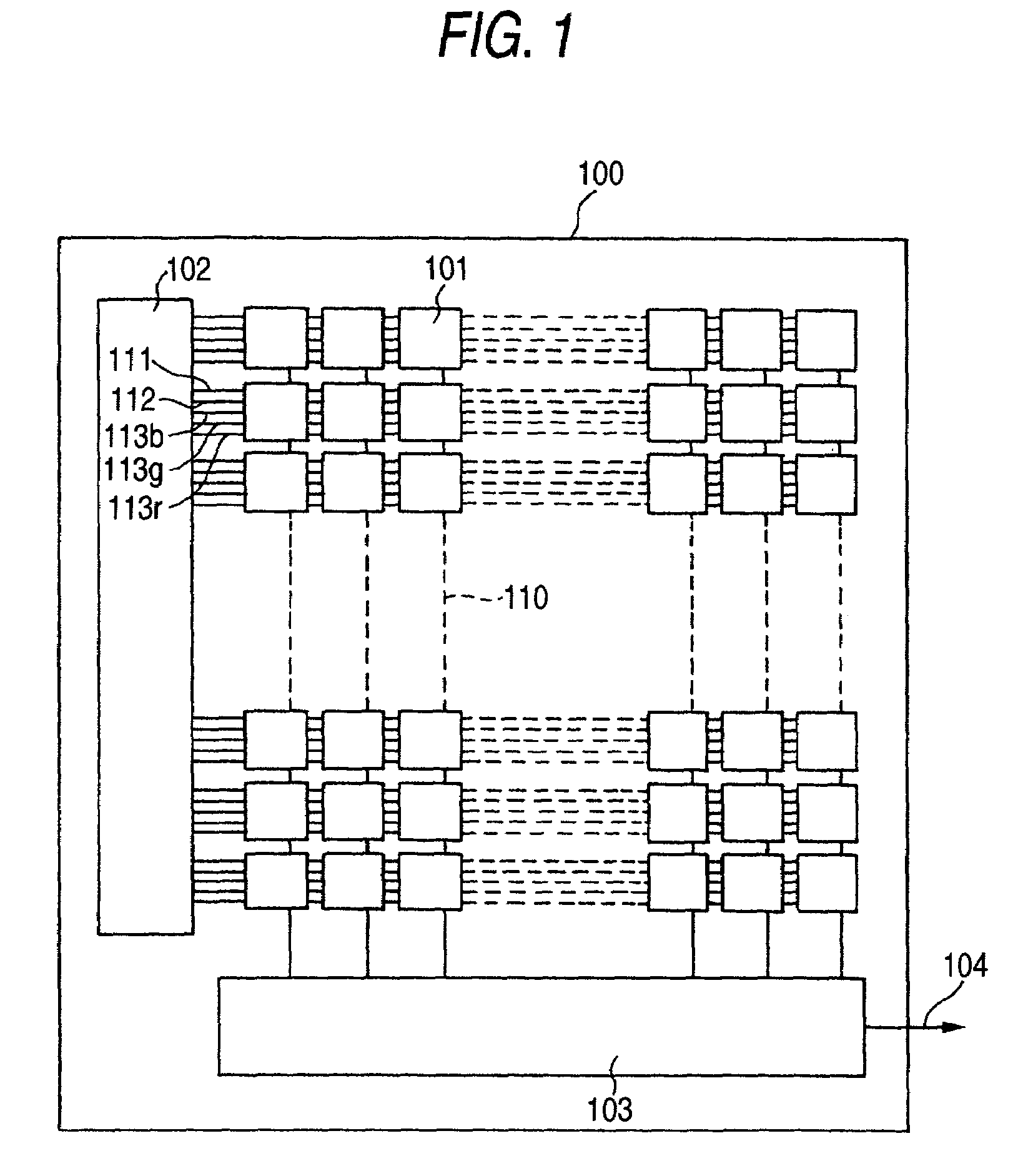
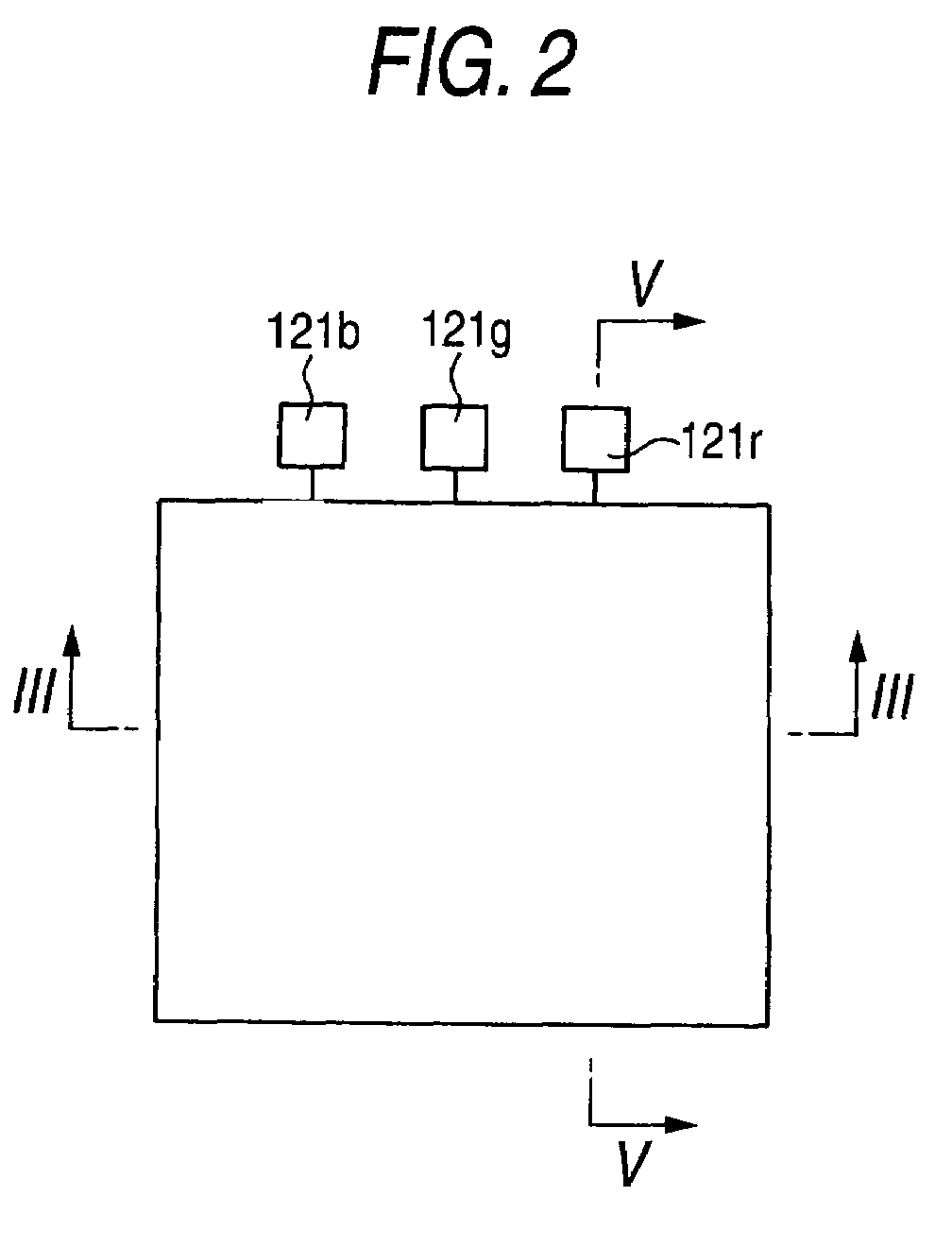
[0051]FIG. 1 is a typical view showing a surface of a solid-state imaging device according to a first embodiment of the invention. The solid-state imaging device 100 includes a large number of photo acceptance portions 101 (each corresponding to a pixel). In this embodiment, the photo acceptance portions 101 are arranged in the form of a tetragonal lattice. Signal readout circuits constituted by an MOS transistor circuit, which will be described later, are formed on a surface portion of a semiconductor substrate under each of the photo acceptance portions 101 of the solid-state imaging device 100.
[0052]Color selection signals through color selection signal lines 113r, 113g and 113b as well as a row selection signal through a row selection signal line 111 and a reset signal through a reset signal line 112 are given from a row selection scanning circuit 102 to each of the signal readout circuits provided in accordance with the photo acceptance portions. Column signal (i.e. image signa...
second embodiment
[0081]In the first embodiment, the following disadvantage may occur. To capture a still image, a mechanical shutter has to be used. If an image signal is output after the mechanical shutter is closed after the image capturing, no problem will be caused. A problem will be, however, caused when the mechanical shutter cannot be used, for example, when a motion picture is captured.
[0082]In the state where signal charges in a certain color pixel become excessive because of a very bright subject, the excessive charges flow into a gate of an output transistor through a color selection transistor. Because the excessive charges are added to any other color signal, color mixture may occur to thereby result in deterioration in image quality.
[0083]Such excessive charges may also occur just after resetting. A signal just after resetting is a reference signal in a zero signal state. The level of the reference signal becomes large. For this reason, there occurs a phenomenon that the level of a sat...
third embodiment
[0086]FIG. 7 is a circuit configuration diagram of each signal readout circuit according to a third embodiment of the invention. This embodiment has the same fundamental circuit configuration as that of FIG. 4 used in the first or second embodiment, but is different from the first or second embodiment in that charge drain transistors 150r, 150g and 150b are added.
[0087]A source of the charge drain transistor 150r is connected to the connection portion 119r. A gate and a drain of the charge drain transistor 150r are connected to the DC power supply line 114. The same rule applies to the charge drain transistors 150g and 150b. Sources of the charge drain transistors 150g and 150b are connected to the connection portions 119g and 119b respectively. Gates and drains of the charge drain transistors 150g and 150b are connected to the DC power supply line 114.
[0088]The film thickness of the gate electrode of each of the charge drain transistors 150r, 150g and 150b and the impurity distribu...
PUM
 Abstract
Description
Claims
Application Information