Antenna element and a method for manufacturing the same

a technology of foil elements and elements, applied in the direction of radiating elements, substantially flat resonant elements, resonant antennas, etc., can solve the problems of significant production cost, difficulty in making the shape of foil elements remain exactly right during fastening, and inconvenient use, so as to avoid waste of resources and reduce manufacturing costs. , the effect of wide area

Inactive Publication Date: 2007-05-15
PULSE FINLAND
View PDF10 Cites 50 Cited by
  • Summary
  • Abstract
  • Description
  • Claims
  • Application Information

AI Technical Summary

Benefits of technology

[0008]The invention has the advantage that a relatively wide area “invisible” at the operating frequencies of the radiating branches of the antenna can be formed between the branches by the customary laser technique. This means lower manufacturing costs compared to the use of the etching process. In addition, the cost of problem waste handling is avoided, which sort of wastes are the chemicals released in the etching process. The invention also has the advantage that the conductor area remaining between the radiating branches can be utilized as an additional radiator on the frequency range of 2.4 GHz, for example.

Problems solved by technology

The difficulty is to make the shape of the foil element remain exactly right during fastening.
Even a relatively small change in the dimensions of especially the non-conductive area of the plane impairs the characteristics of the antenna significantly.
The chemicals needed in the process cause a considerable cost in production.
This drawback is emphasized if the area between the conductor branches is made relatively wide in order to increase the bandwidths of the antenna.
Besides, the chemicals used are environmental poisons, the disposal of which causes additional costs.
Removing a relatively wide conductor area would thus be impractical, i.e. expensive, and it would also impair the mechanical and electrical characteristics of the dielectric plate used as a substrate.

Method used


Image

  • Antenna element and a method for manufacturing the same
  • Antenna element and a method for manufacturing the same
  • Antenna element and a method for manufacturing the same

Examples


Embodiment Construction

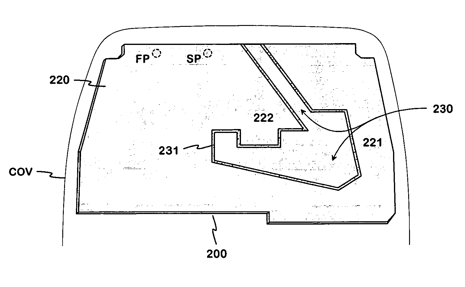
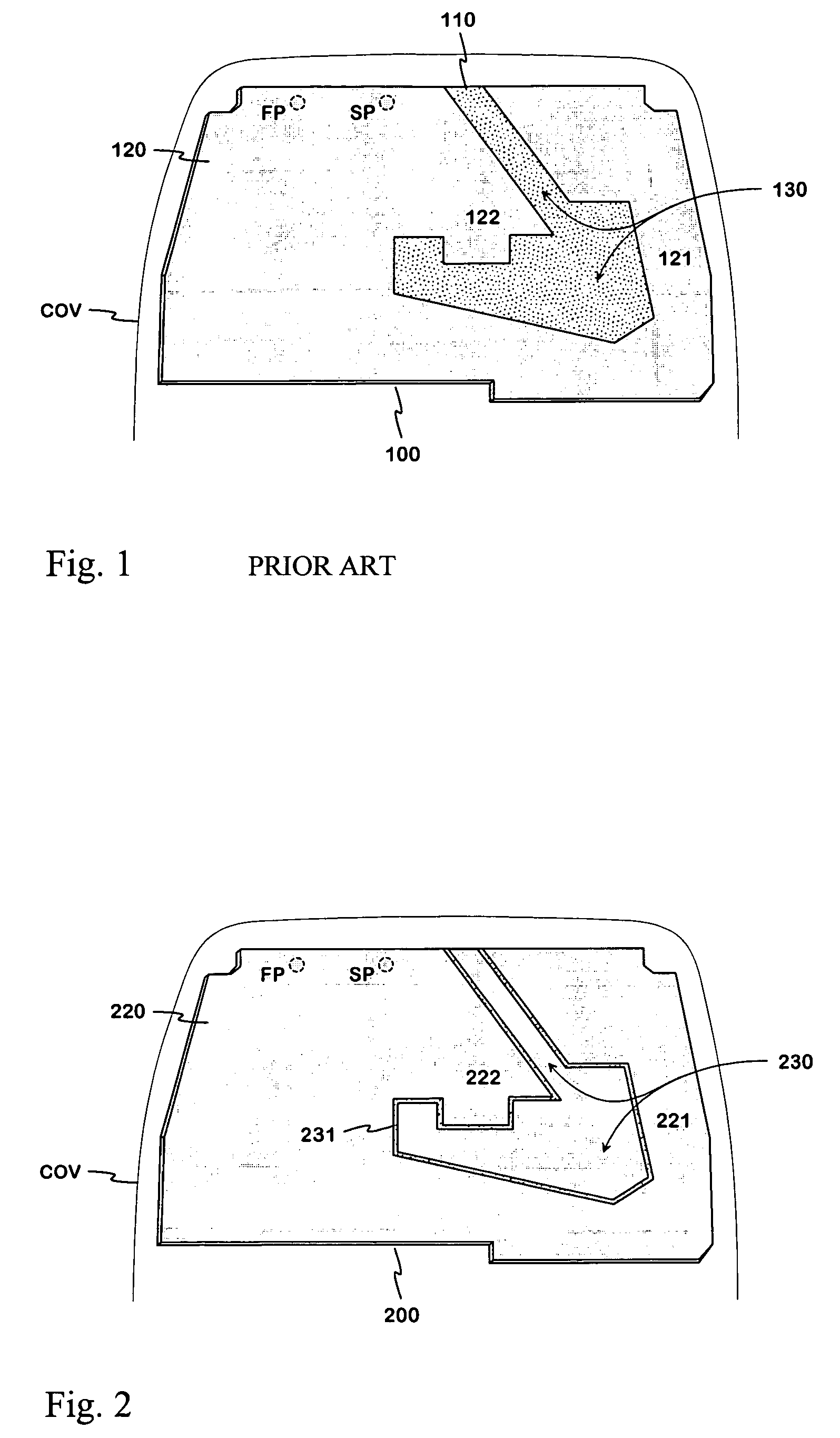
[0019]FIG. 2 shows an example of a radiating antenna element according to the invention. The antenna element 200 comprises a dielectric substrate and a radiating plane 220 on its surface, divided into two conductor branches, like in the element of FIG. 1. The elements differ from each other with respect to the area separating the radiating conductor branches. In FIG. 1, the conductive coating has been entirely removed from that intermediate area 130. In FIG. 2 again, the original conductive coating is almost entirely left on the corresponding intermediate area 230. The conductive coating has been only narrowly removed at the border line of the intermediate area. The line-like non-conductive area thus created is called a “groove”. So, the intermediate area 230 is confined by a border groove 231. The conductor area remaining inside the border groove, which is slightly smaller than the intermediate area 230, forms in the complete product, in principle, together with the ground plane an...


PUM


Abstract

A radiating antenna element intended for small-sized radio devices and a method for manufacturing the same. The element (300) is manufactured of a plate comprising a dielectric substrate coated with conductive material on one side. The radiating conductor branches corresponding to the operating bands of the antenna are formed on the plate by removing the conductive coating by laser narrowly from the border line of the area (330) between the designed conductor branches. The conductor area confined by the created border groove can be used as a parasitic additional radiator. If needed, the conductor area confined by the border groove (331) can also be split into a number of small conductor areas (CA1, CA2), in order to make sure that the conductor area does not radiate or have any substantial effect on the coupling between the radiating conductor branches. A relatively wide area “invisible” on the operating frequencies of the radiating branches of the antenna can be formed between the branches by the customary laser technique. This means lower manufacturing costs compared to the use of the etching process, and the creation of problem waste is also avoided.

Description

[0001]The invention relates to a radiating antenna element intended particularly for small-sized radio devices. The invention also relates to a method for manufacturing an antenna element according to it.BACKGROUND OF THE INVENTION[0002]An internal antenna is generally used in small-sized radio devices, such as mobile phones, in order to avoid a part protruding from the cover of the device. Internal antennas are usually planar antennas, because they have relatively good electric properties. A planar antenna comprises a radiating plane and a ground plane parallel with it. The planes are generally connected to each other by a short-circuit conductor because of the matching of the antenna. The structure is dimensioned so that it functions as a resonator at the operating frequency, which is a prerequisite for effective radiation. In modern mobile stations it is a normal requirement that the antenna must operate on two different frequency bands, in which case two resonators are also requ...

Claims


Application Information

Patent Timeline
Patent Type & Authority Patents(United States)
IPC IPC(8): H01Q1/38H01Q5/00H01Q5/371H01Q5/378H01Q9/04
CPCH01Q1/38H01Q9/0407H01Q5/378H01Q5/371H01Q9/0442
Inventor ANNAMAA, PETTERINIEMI, MATTIANTILA, KIMMONIEMELA, ILKKA
Owner PULSE FINLAND
Why Eureka
Try Eureka