Active matrix organic light emitting display panel

a technology of organic light and display panel, applied in the direction of instruments, discharge tube luminescnet screens, static indicating devices, etc., can solve the problems of small limit in how much the width or thickness of the power line could be increased to keep the voltage drop small, and large difference between voltages applied to pixels connected respectively to the first and last stages of the power line to achieve the effect of reducing the voltage drop across the power lin

Active Publication Date: 2007-05-22
LG DISPLAY CO LTD
View PDF3 Cites 5 Cited by
  • Summary
  • Abstract
  • Description
  • Claims
  • Application Information

AI Technical Summary

Benefits of technology

[0018]An object of the present invention is to provide an active matrix organic light emitting display panel that has a structure in which a routing line of a power line is extended in width into a seal pattern portion and the extended portion of the routing line is of a mesh type, thereby making it possible to reduce a voltage drop across the power line.

Problems solved by technology

Cathode ray tube (CRT) has drawbacks due to its heavy weight and large volume.
Yet, due to the structure of the active-matrix organic light emitting display panel according to the related art, there is a limit in how much the width or thickness of the power line could be increased for keeping the voltage drop across the power line small.
Accordingly, a large voltage drop across the power line cannot be avoided, thereby causing a large difference between voltages applied to pixels connected respectively to the first and last stages of the power line.
Thus, an image quality of the organic light emitting display according to the related art is not uniformly maintained.
However, since the routing line is formed in the non-display region, and the non-display region of the panel is kept small to maximize the display region, the structure of the active-matrix organic light emitting display panel according to the related art cannot sufficiently increase the width or thickness of the power line.
Thus, the organic light emitting display according to the related art has a large voltage drop across the power line and is unable to uniformly maintain the image quality.

Method used


Image

  • Active matrix organic light emitting display panel
  • Active matrix organic light emitting display panel
  • Active matrix organic light emitting display panel

Examples


Embodiment Construction

[0031]Reference will now be made in detail to the preferred embodiments of the present invention, examples of which are illustrated in the accompanying drawings.

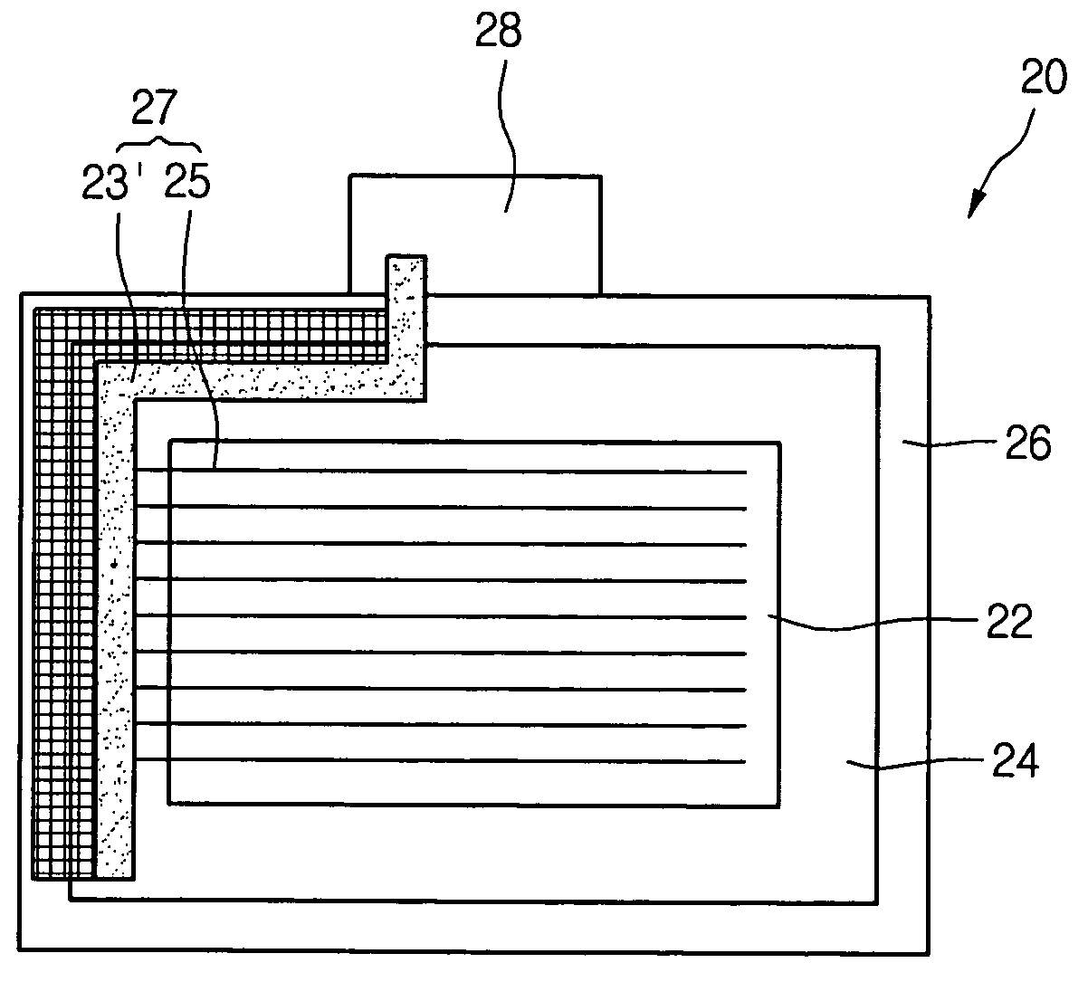
[0032]FIGS. 4A and 4B are schematic plan views illustrating a power line of an active matrix organic light emitting display panel according to an embodiment of the present invention. As shown in FIGS. 4A and 4B, an active matrix organic light emitting display panel includes a substrate 20. The substrate 20 may be a lower substrate or an upper substrate of the organic light emitting display panel, and may be attached to a second substrate (not shown). The substrate 20 and the second substrate (not shown) may be encapsulated to prevent moisture and oxygen from infiltrating into the active-matrix organic light emitting display panel. For example, a sealant may be coated in a seal pattern portion 26 of the substrate 20 for attaching the substrate 20 with the second substrate (not shown). Alternatively, the sealant may be coated ...


PUM


Abstract

An active matrix organic light emitting display panel includes a first substrate including a seal pattern region, a non-display region, and a display region, the non-display region being between the display region and the seal pattern region, a pad connected to the first substrate, and a power line including a routing line connected directly to the pad, and a pixel line for applying a pixel voltage to a plurality of pixels, the routing line having a first portion being in the non-display region and a second portion being in the seal pattern region, and the pixel line being in the display region.

Description

BACKGROUND OF THE INVENTION[0001]1. Field of the Invention[0002]The present invention relates to an organic light emitting display panel, and more particularly, to an active matrix organic light emitting display panel having a structure capable of minimizing a resistance of a power line.[0003]2. Discussion of the Related Art[0004]Cathode ray tube (CRT) has drawbacks due to its heavy weight and large volume. Thus, many efforts have been made to research and develop various flat display devices, such as liquid crystal display (LCD) devices, field emission display (FED) devices, plasma display panel (PDP) devices, and organic light emitting display devices, which is also often referred to as organic electro luminescent display devices, as a substitute for CRT devices.[0005]An organic light emitting display device is a self-luminescent type display. In general, the organic light emitting display device emits light by injecting electrons from a cathode and holes from an anode into an emi...

Claims


Application Information

Patent Timeline
Patent Type & Authority Patents(United States)
IPC IPC(8): H05B33/00H01L29/04
CPCG09G3/3208H01L27/3279H01L51/5246G09G2320/0233H10K59/1315H10K50/8426
Inventor OH, DU HWANCHUNG, HOON JU
Owner LG DISPLAY CO LTD
Why Eureka
Try Eureka