Processes for forming backplanes for electro-optic displays

a backplane and electrooptic technology, applied in the field of electrooptic (electronic) display backplane forming process, can solve the problems of not being bistable, preventing widespread use of these displays, and operating in a transmissive mod

Inactive Publication Date: 2007-05-29
E INK CORPORATION
View PDF131 Cites 267 Cited by
  • Summary
  • Abstract
  • Description
  • Claims
  • Application Information

AI Technical Summary

Benefits of technology

[0031]Alternatively, after formation of a plurality of backplanes, the flexible substrate may be separated from the substantially rigid carrier, and thereafter the flexible substrate separated into a plurality of separate sections, each comprising one backplane. In such a process, after separation of the substantially rigid carrier from the flexible substrate but before separation of the flexible substrate into the sections, the flexible substrate may have an electrical connector to each of the backplanes, and / or an electro-optic medium may be deposited on the backplanes. Again, separation of the substantially rigid carrier from the backplane is conveniently effected by radiation ablation of an ablatable layer disposed between the substantially rigid carrier and the backplane, and a supporting layer may be attached to the flexible substrate after separation of the flexible substrate from the substantially rigid carrier.

Problems solved by technology

Nevertheless, problems with the long-term image quality of these displays have prevented their widespread usage.
For example, particles that make up electrophoretic displays tend to settle, resulting in inadequate service-life for these displays.
Liquid crystals, including polymer-dispersed liquid crystals, are, of course, also electro-optic media, but are typically not bistable and operate in a transmissive mode.
Fabrication processes, however, can result in significant cost.
However, manufacturing flexible microelectronic backplanes for such displays presents many challenges.
This is problematic for two reasons.
Secondly, a substantial investment by an existing display manufacturer will be required.
After retrofitting a fab for flexible substrates, it may not be possible to simultaneously process glass substrates due to the differences in the fixtures required.
Thick steel substrates may not require as much specialized tooling for handling; however, display manufacturers may still be hesitant to process steel substrates due to contamination concerns and other issues.
In any case, display manufacturers may be unwilling to make the required investment during the early stages of flexible display development.

Method used


Image

  • Processes for forming backplanes for electro-optic displays
  • Processes for forming backplanes for electro-optic displays
  • Processes for forming backplanes for electro-optic displays

Examples


Embodiment Construction

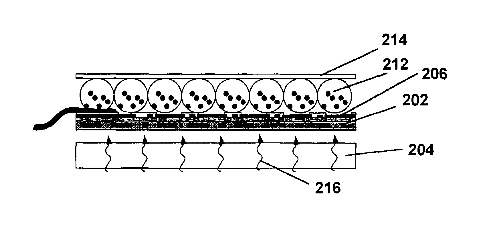
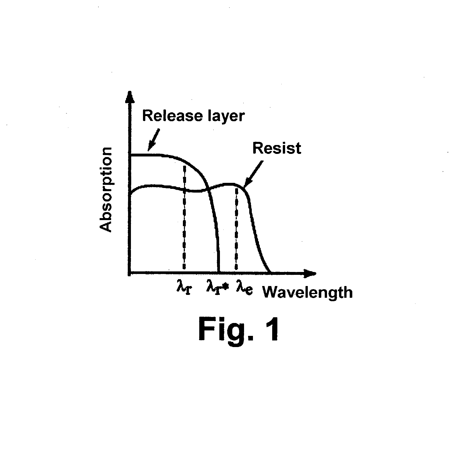
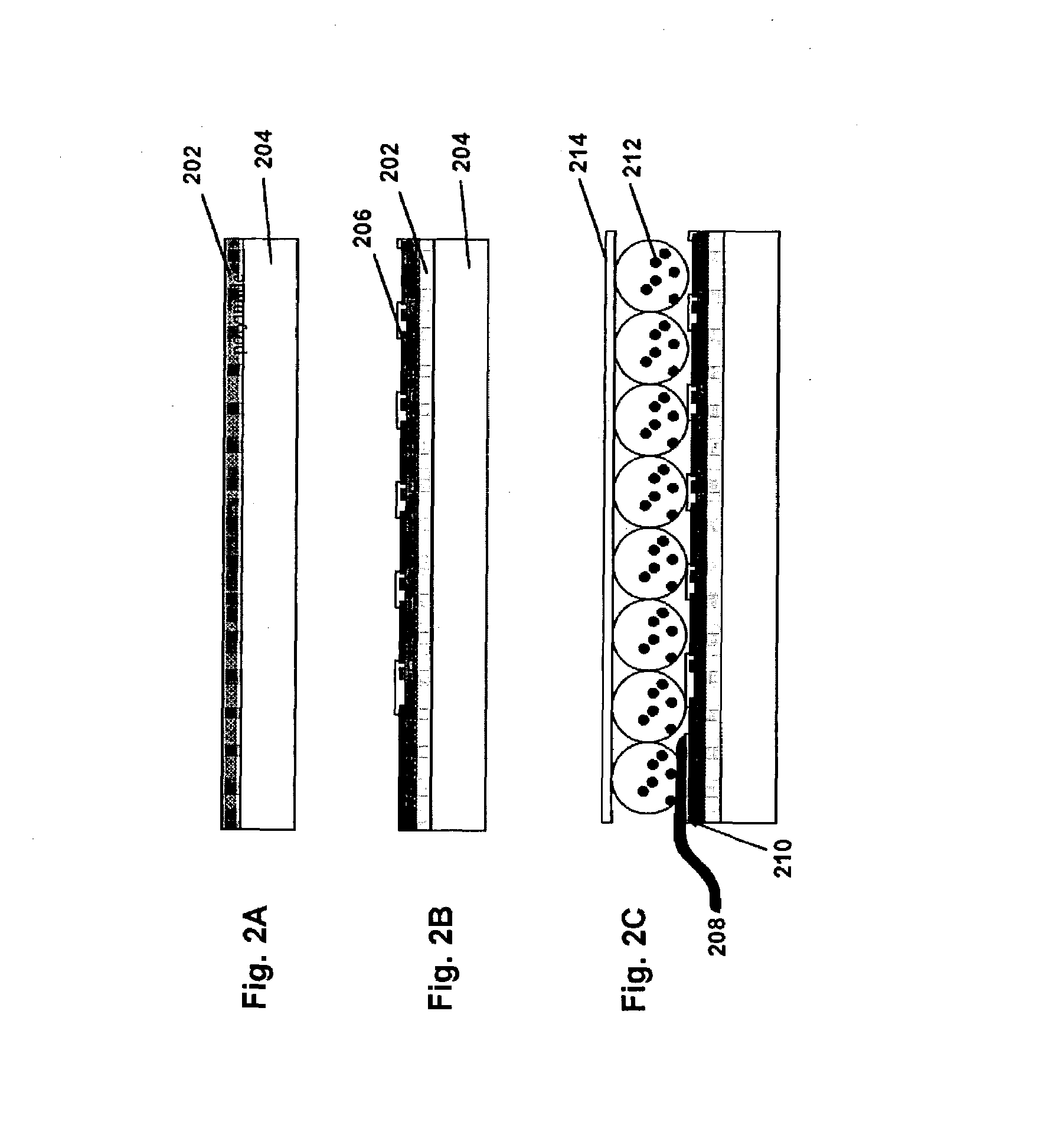
[0062]In the following detailed description, rigid carrier processes of the invention will first be described with reference to FIGS. 1–10B. Next, processes for the formation of transistors by processes of the invention will be described with reference to FIGS. 11–17. Processes of the invention for the formation of diodes and diode arrays will then be described with reference to FIGS. 18A–21. Finally, methods of the present invention for driving electro-optic displays will be described.

Rigid Carrier Processes

[0063]As already mentioned this invention provides a rigid carrier process for forming a non-linear element, which may be a diode or a transistor, on a flexible substrate. The flexible substrate is secured to a substantially rigid carrier, at least one non-linear element is formed on the flexible substrate, and then the flexible substrate and the at least one non-linear element are separated from the substantially rigid carrier.

[0064]In the rigid carrier process of the present i...


PUM

PropertyMeasurementUnit
temperaturesaaaaaaaaaa
exposure wavelength λeaaaaaaaaaa

Abstract

A non-linear element is formed on a flexible substrate by securing the substrate to a rigid carrier, forming the non-linear element, and then separating the flexible substrate from the carrier. The process allows flexible substrates to be processed in a conventional fab intended to process rigid substrates. In a second method, a transistor is formed on a insulating substrate by forming gate electrodes, depositing a dielectric layer, a semiconductor layer and a conductive layer, patterning the conductive layer to form source, drain and pixel electrodes, covering the channel region of the resultant transistor with an etch-resistant material and etching using the etch-resistant material and the conductive layer as a mask, the etching extending substantially through the semiconductor layer between adjacent transistors. The invention also provides a process for forming a diode on a substrate by depositing on the substrate a first conductive layer, and a second patterned conductive layer and a patterned dielectric layer over parts of the first conductive layer, and etching the first conductive layer using the second conductive layer and dielectric layer as an etch mask. Finally, the invention provides a process for driving an impulse-sensitive electro-optic display.

Description

CROSS REFERENCE TO RELATED APPLICATIONS[0001]This application claims priority from Application Ser. No. 60 / 375,246, filed Apr. 24, 2002 and Application Ser. No. 60 / 376,603, filed Apr. 30, 2003. This application is also related to application Ser. No. 09 / 565,413, filed May 5, 2000; application Ser. No. 09 / 904,109, filed Jul. 12, 2001 (Publication No. 2002 / 0106847, now U.S. Pat. No. 6,683,333); copending application Ser. No. 09 / 904,435, filed Jul. 12, 2001 (Publication No. 2002 / 0060321), and copending application Ser. No. 10 / 065,795, filed Nov. 20, 2002 (Publication No. 2003 / 0137521). This application is also related to copending application Ser. No. 10 / 249,618, of even date herewith, entitled “Backplanes for display applications, and components for use therein” (Publication No. 2003 / 0222315). The entire contents of the aforementioned applications are herein incorporated by reference. The entire contents of all United States Patents and published Applications mentioned below are also ...

Claims


Application Information

Patent Timeline
Patent Type & Authority Patents(United States)
IPC IPC(8): H01L21/30B60C23/04G02F1/1333G02F1/1362G02F1/167H01L21/336H01L29/786
CPCB60C23/04G02F1/1362G02F1/167H01L27/1214H01L27/1266H01L29/66765H01L29/78603H01L27/1288G02F1/133305G02F2001/13613G02F1/13613
Inventor KAZLAS, PETER T.KANE, NATHAN R.RITENOUR, ANDREW P.
Owner E INK CORPORATION
Why Eureka
Try Eureka