Display apparatus and method of manufacturing the same

Active Publication Date: 2007-05-29
JOLED INC
View PDF20 Cites 46 Cited by
  • Summary
  • Abstract
  • Description
  • Claims
  • Application Information

AI Technical Summary

Benefits of technology

[0017]According to the display apparatus and the manufacturing method thereof according to the present invention, the auxiliary wiring connected to the upper electrode is composed of the same layer as that formed in the same step as that for forming the lower electrodes, whereby a display apparatus with a small pixel pitch in which the electric resistance of the upper electrode is lo

Problems solved by technology

Therefore, the upper electrode is required to be thinned for securing a light-transmitting property, which tends to raise resistance value, thereby easily causing a voltage drop.
In the display apparatus having the auxiliary wiring in the configuration shown in Patent Reference 1, however, a special layer for forming the auxiliary wiring is provided, leading to a complication of the layer structure in the dis

Method used


Image

  • Display apparatus and method of manufacturing the same
  • Display apparatus and method of manufacturing the same
  • Display apparatus and method of manufacturing the same

Examples


Embodiment Construction

[0025]Now, the display apparatus and the manufacturing method thereof according to the present invention will be described in detail below referring to the drawings.

1>

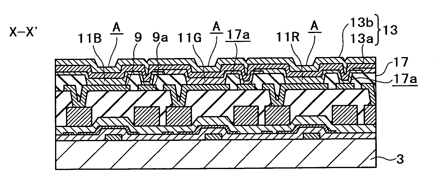
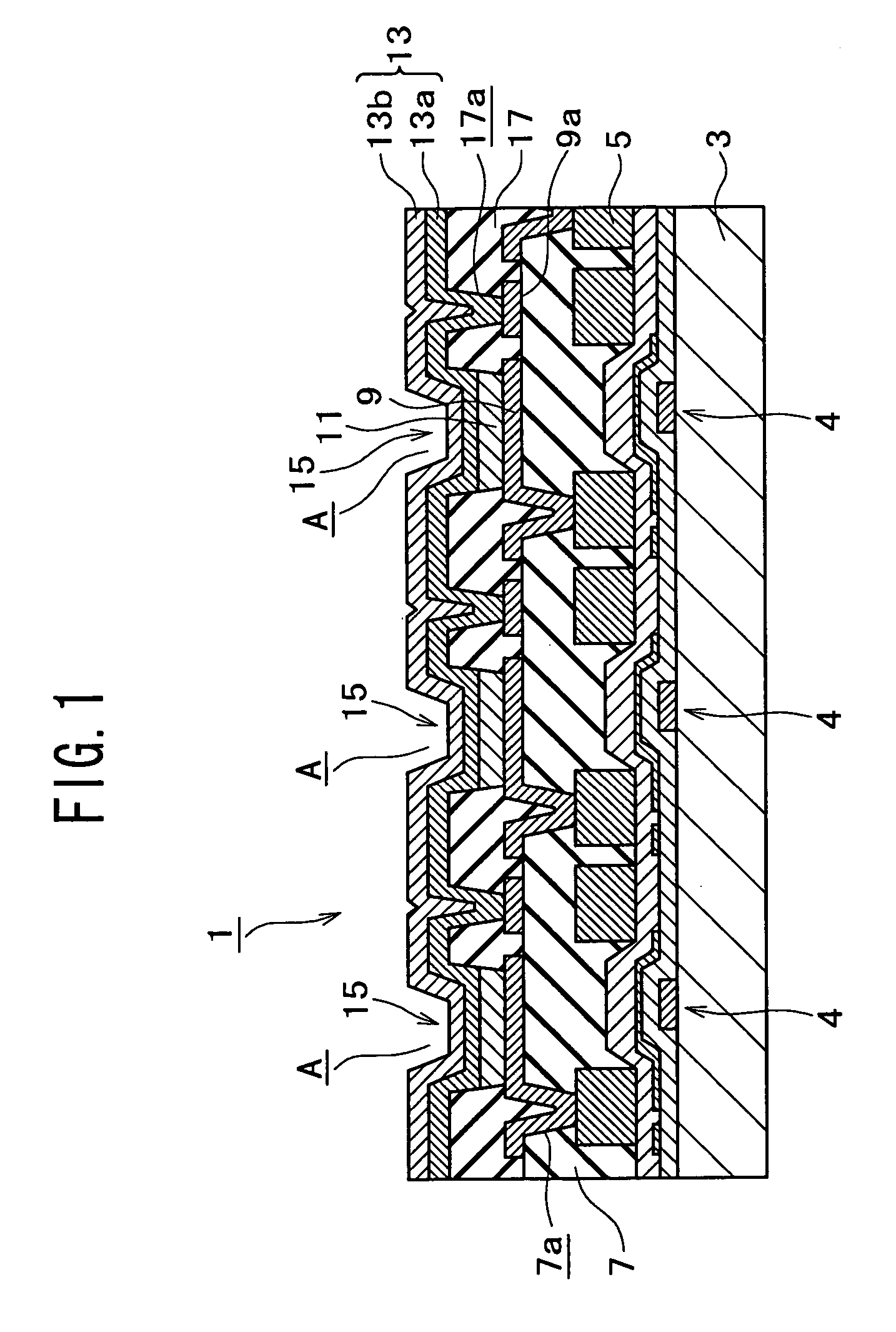
[0026]FIG. 1 is a sectional view of an essential part showing the general configuration of a display region in a display apparatus according to a first embodiment of the present invention. The display apparatus 1 shown in the figure is an active matrix type display apparatus in which organic EL devices are arranged as light-emitting devices.

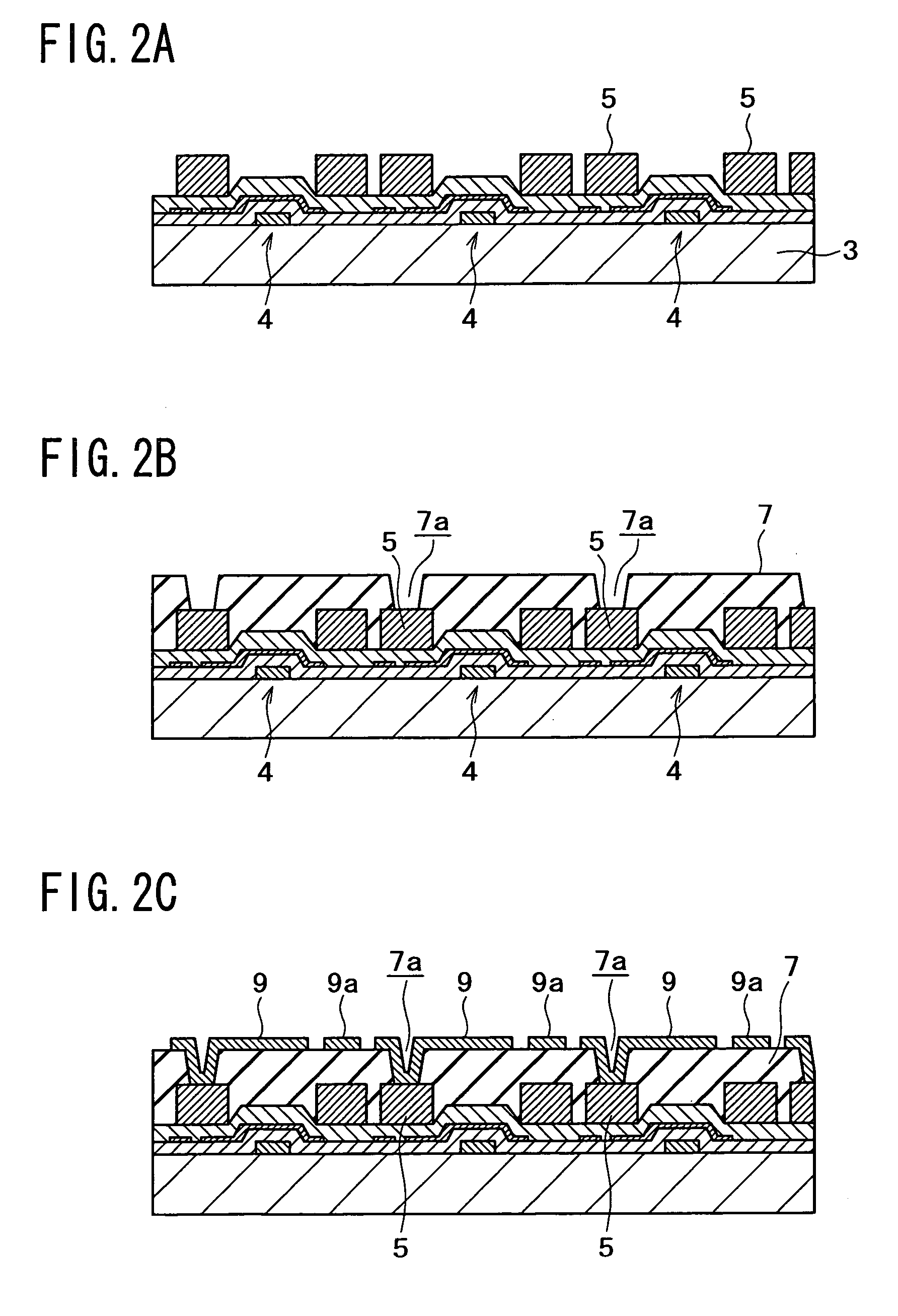
[0027]The display apparatus 1 comprises thin film transistors (hereinafter referred to as TFT) 4 at each pixel on a substrate 3. On the substrate 3 provided thereon with the TFTs 4, a wiring 5 connected to the source / drain of the TFTs 4 is formed, and a planarizing insulation film 7 is provided in the state of covering the wiring 5. The TFT 4 is not limited to the bottom gate type shown, and may be of the top gate type, and its gate electrode is connected to a scan circuit.

[0028]An ...


PUM

PropertyMeasurementUnit
Structureaaaaaaaaaa
Lightaaaaaaaaaa
Reflectionaaaaaaaaaa

Abstract

Disclosed is a display apparatus including a plurality of lower electrodes patterned on a substrate on the basis of each pixel, an auxiliary wiring composed of the same layer as the lower electrodes and arranged in the state of being insulated from the lower electrodes, an insulating film formed on the substrate and provided with pixel openings for exposing central portions of the lower electrodes and connection holes reaching the auxiliary wiring, organic layers so patterned as to cover bottom portions of the pixel openings and to have end portions partly overlapping on each other between the adjacent pixels, and an upper electrode so formed as to cover the organic layers and to be connected to the auxiliary wiring through the connection holes between the organic layers. Also disclosed is a method of manufacturing the display apparatus.

Description

RELATED APPLICATION DATA[0001]The present application claims priority to Japanese Application(s) No(s). P2002-358895 filed Dec. 11, 2003, and P2003-283527 filed Jul. 31, 2003, which application(s) is / are incorporated herein by reference to the extent permitted by law.BACKGROUND OF THE INVENTION[0002]The present invention relates to a display apparatus including organic electroluminescence devices each of which comprises an organic light emission layer, and a method of manufacturing the same.[0003]An organic electroluminescence device utilizing electroluminescence (hereinafter referred to as EL) of an organic material comprises an organic layer composed of a lamination of an organic hole transport layer and an organic light emission layer between a lower electrode and an upper electrode, and has drawn attention as a light emitting device capable of high-luminance light emission when driven by a low-voltage DC current.[0004]An active matrix type display apparatus using such organic EL...

Claims


Application Information

Patent Timeline
IPC IPC(8): H01L51/00H05B33/26G09F9/00G09F9/30H01J1/62H01J63/04H01L21/3205H01L23/52H01L27/32H01L51/50H01L51/52H05B33/10H05B33/12H05B33/14H05B33/24H05B33/28
CPCH01L27/3276H01L51/5234H01L51/5228H01L27/3258H01L51/5218Y10S428/917H01L2251/5315H10K59/124H10K59/131H10K50/818H10K50/824H10K50/828H10K2102/3026H05B33/26
Inventor SATO, CHIYOKOYAMADA, JIROHIRANO, TAKASHIYOKOYAMA, SEIICHI
Owner JOLED INC
Why Eureka
Try Eureka