Semiconductor integrated circuit device and its manufacture using automatic layout

a technology of integrated circuit devices and layouts, applied in the direction of cad circuit design, program control, instruments, etc., can solve the problems of wasteful space likely to be formed, affecting the effective use of substrate areas, and forming wasteful space in substrate areas, etc., to achieve high integration density

Inactive Publication Date: 2007-06-05
YAMAHA CORP
View PDF6 Cites 108 Cited by
  • Summary
  • Abstract
  • Description
  • Claims
  • Application Information

AI Technical Summary

Benefits of technology

[0012]Another object of this invention is to provide a semiconductor integrated circuit device capable of automatic layout and an improved integration density.
[0013]Still another object of this invention is to provide a manufacture method for a semiconductor integrated circuit device capable of eliminating a wasteful space as much as possible by automatic layout and effectively using a substrate area.
[0018]As above, the shape of a shape-variable wiring region is determined based upon cell layout information and wiring information and a wiring pattern is determined automatically. Accordingly, the area of an integrated circuit can be effectively used and a high integration density can be attained.

Problems solved by technology

If the height is fixed, wasteful space is likely to be formed so that the effective use of a substrate area may be hindered.
However, a wasteful space is formed in the substrate area if the numbers of wirings in cells along a column are large in some cells and small in some cells or by other reasons.

Method used


Image

  • Semiconductor integrated circuit device and its manufacture using automatic layout
  • Semiconductor integrated circuit device and its manufacture using automatic layout
  • Semiconductor integrated circuit device and its manufacture using automatic layout

Examples


Embodiment Construction

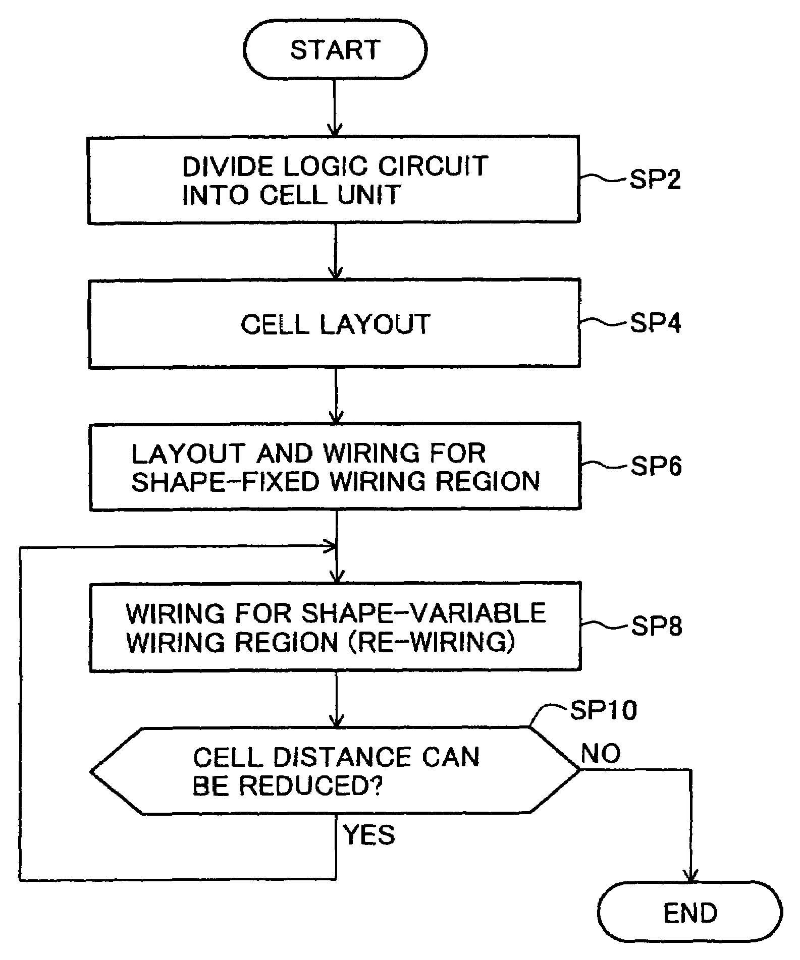
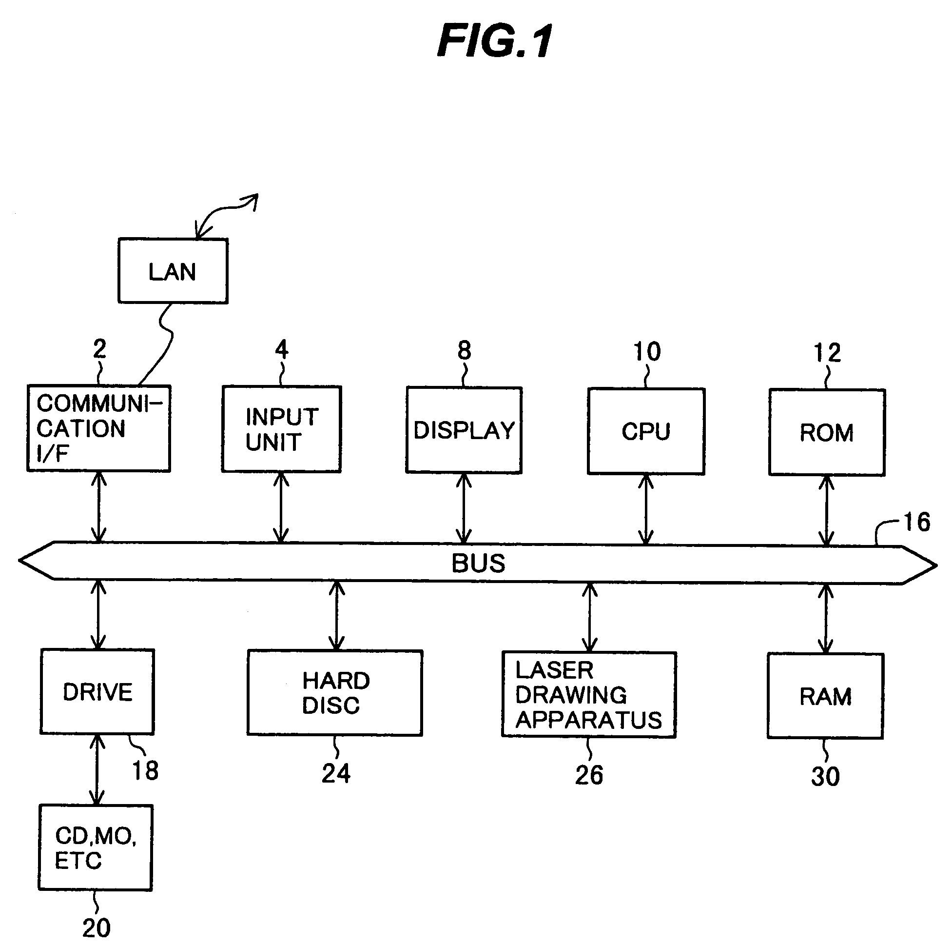
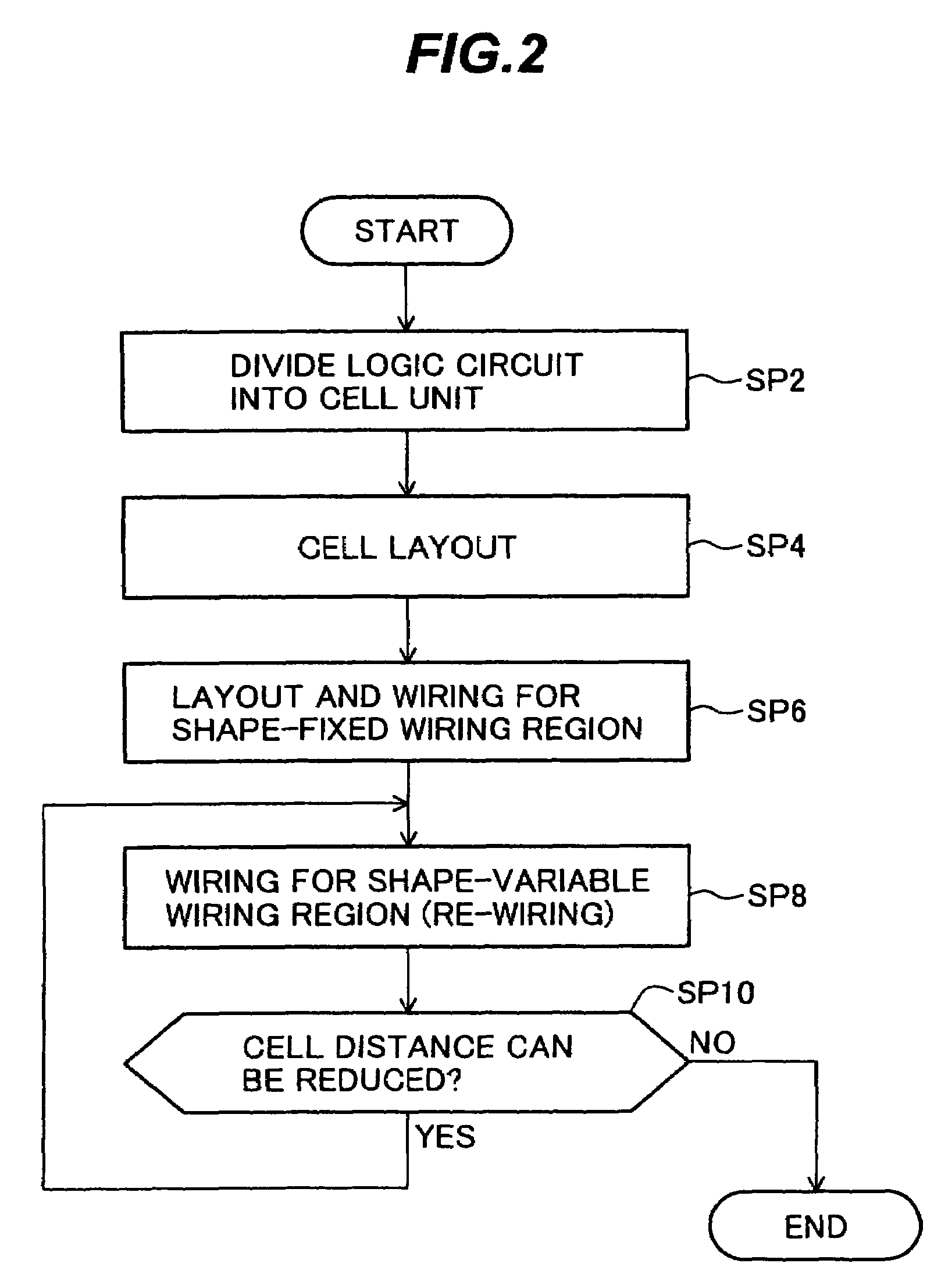
[0025]With reference to FIG. 1, the structure of an automatic layout wiring system will be described. The automatic layout wiring system is made of a general computer and an application program to be run on the general computer.

[0026]Referring to FIG. 1, a communication interface 2 is used for transferring layout wiring data and the like to and from another system via a local area network (LAN). An input unit 4 may be an alphanumeric input keyboard, a mouse, a pattern drawing digitizer or the like. A display unit 8 displays various information for users. A CPU 10 performs logical computation in accordance with a program and controls other constituent units via a bus 16. A ROM 12 stores an initial program loader and the like of the automatic layout wiring system. A removable disk drive 18 performs data read / write of a removable disk 20 such as CD-ROM, MO and the like.

[0027]A hard disk 24 stores an operating system for the computer, application programs, layout wiring data and the lik...


PUM


Abstract

A semiconductor integrated circuit device has: a semiconductor substrate defining a plurality of rows, each row including areas for a sequence of cells; a plurality of active regions disposed in each of the rows constituting semiconductor elements of associated cells; and a wiring region of stripe shape elongated along a direction of row, defined on the semiconductor substrate outside of the active regions in each row, and including wirings belonging to the associated cells, each wiring region having height in a direction crossing the row direction, the wiring region having locally different height.

Description

RELATED APPLICATIONS[0001]This application is a divisional application of U.S. patent application Ser. No. 10 / 697,074, filed Oct. 30, 2003.CROSS REFERENCE TO RELATED APPLICATION[0002]This application is based on and claims priority of Japanese Patent Application No. 2002-316997 filed on Oct. 31, 2002, the entire contents of which are incorporated herein by reference.BACKGROUND OF THE INVENTION[0003]A) Field of the Invention[0004]The present invention relates to a semiconductor integrated circuit device and its manufacture, and more particularly to a semiconductor integrated circuit device capable of being designed with automatic layout and its manufacture.[0005]B) Description of the Related Art[0006]It is desired to develop in a short time semiconductor integrated circuit devices of various types and small quantity. A semiconductor integrated circuit device can be designed by automatic layout using a computer. In a standard cell method, patterns of basic gates and frequently used lo...

Claims


Application Information

Patent Timeline
Patent Type & Authority Patents(United States)
IPC IPC(8): G06F17/50H01L21/82H01L27/02H01L27/118H01L29/739
CPCG06F17/5068H01L27/0207H01L27/118H01L27/11807G06F30/39
Inventor ONO, YUKICHI
Owner YAMAHA CORP
Why Eureka
Try Eureka