Scatterometry for samples with non-uniform edges
- Summary
- Abstract
- Description
- Claims
- Application Information
AI Technical Summary
Benefits of technology
Problems solved by technology
Method used
Image
Examples
Embodiment Construction
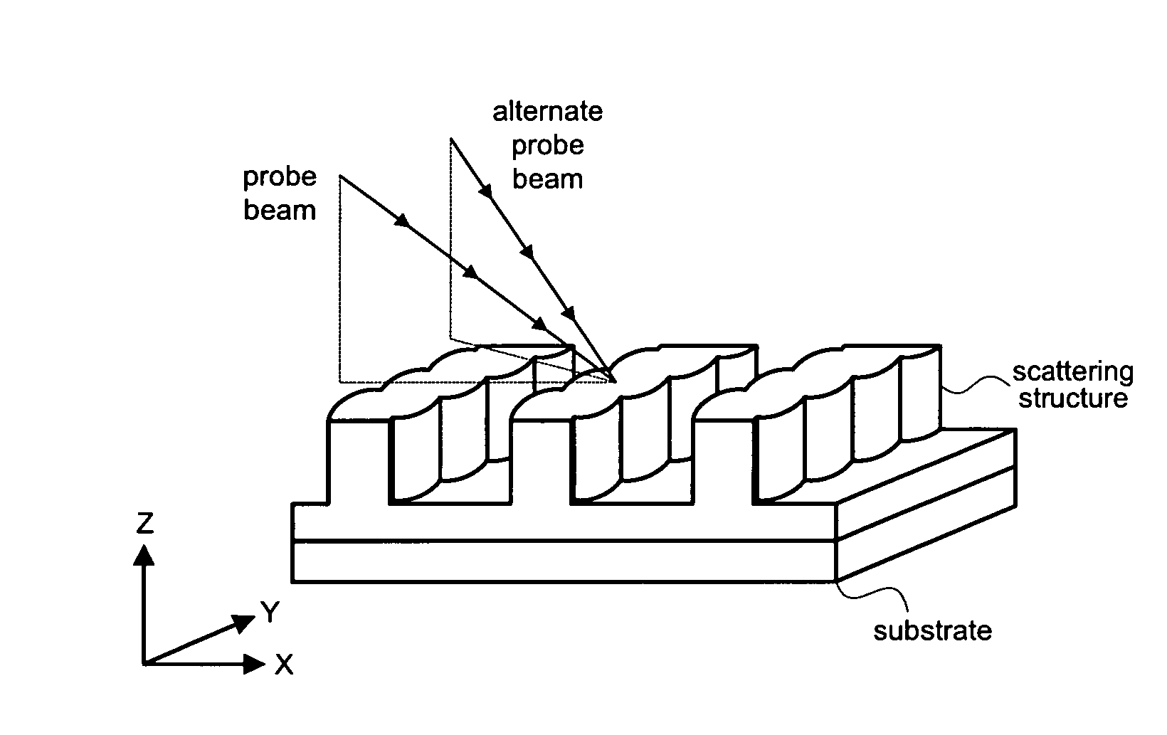
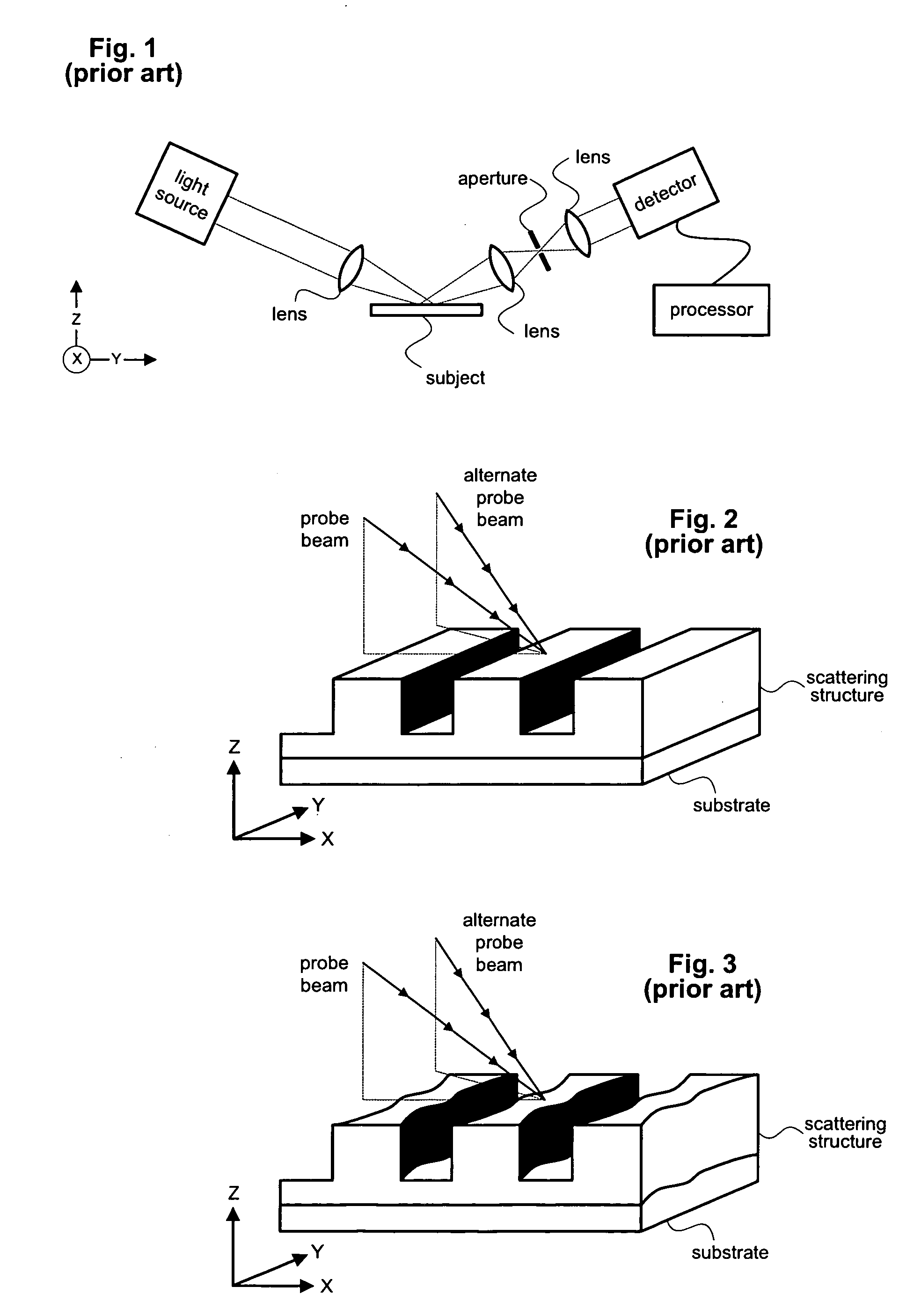
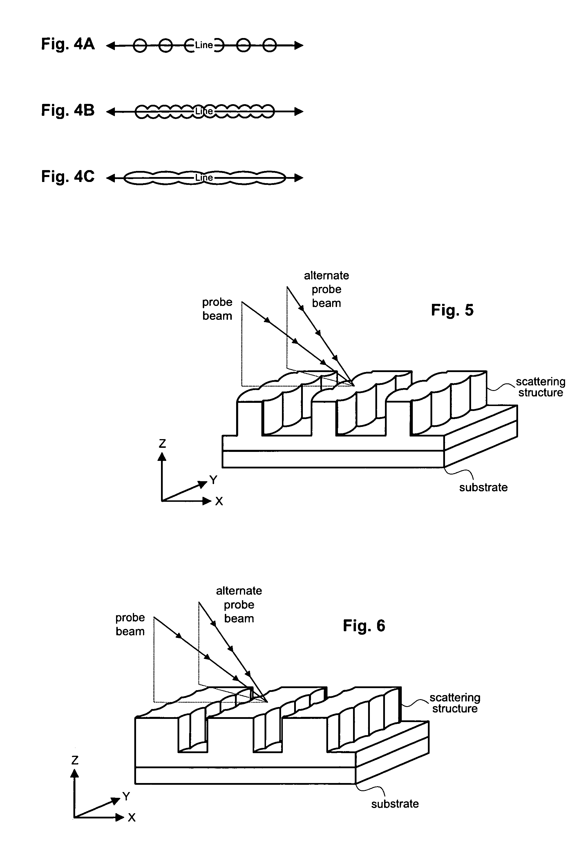
[0028]The present invention provides a method for simulating line edge roughness within optical models of scatterometry samples. For typical applications, the sample is a semiconductor wafer and includes a scattering structure formed on one or more underlying layers. The lowermost of the underlying layers is commonly referred to as a substrate. The scatting structure is covered by an incident medium that is typically air but may be vacuum, gas, liquid, or solid (such as an overlaying layer or layers). In the most typical case, the scattering structure is a grating consisting of a periodic series of lines. By appropriate generalizations, other isolated or periodic features may also be modeled.
[0029]To model roughness, edges within the scattering structure are represented as combinations of three dimensional objects. This is shown, for example, in FIG. 4A where a line is modeled using a series of cylindrical mesas. Each shape (mesa) has the same size and the series of shapes are align...
PUM
 Abstract
Description
Claims
Application Information


