III-nitride compound semiconductor light emitting device

a light-emitting device and compound semiconductor technology, which is applied in the direction of spectacles/goggles, instruments, spectacles/goggles, etc., can solve the problems of mechanical processing, deterioration of film quality, and phenomenon, so as to maximize the external quantum efficiency effectively get out of the light-emitting device, and effective roughness

Inactive Publication Date: 2011-04-12
EPIVALLEY
View PDF38 Cites 1 Cited by
  • Summary
  • Abstract
  • Description
  • Claims
  • Application Information

AI Technical Summary

Benefits of technology

[0018]According to the present invention, the external quantum efficiency of the light emitting device can be maximized by forming an effective roughness on an active layer by the peculiar method of the present invention. This is because the light emitting device according to the present invention has a structure where light emitted from the active layer can be refracted on the roughness surface while effectively getting out of the light emitting device.

Problems solved by technology

One of unavoidable basic problems in the semiconductor light emitting device is that a phenomenon will occur where a significant portion of light generated in the semiconductor light emitting device is entrapped within the semiconductor light emitting device due to a difference in dielectric constant between the semiconductor light emitting device and the surrounding air.
Recently, the surface is also made rough by changing growth conditions, such as pressure, temperature and gas flow, in the growth of the p-type layer, while causing deterioration in the film quality.
The above-mentioned mechanical processing is easy on a substrate, such as SiC, but almost impossible on a sapphire substrate with high strength.
Also, the use of the chemical or dry etching technique has a limitation in area which can be made rough.
Another problem is that the process becomes complicated since an etching process is further added to the existing LED (light emitting diode) process.
Also, there are problems in the reproduction and uniformity of the etching process.
However, in the case of the method of making the surface rough by changing the growth conditions, the deterioration in the thin-film quality is unavoidable.
Accordingly, the growth of a layer with bad quality in more than certain thickness can increase the external quantum efficiency of the light emitting device, but cause a fatal problem in the reliability of the light emitting device.

Method used


Image

  • III-nitride compound semiconductor light emitting device
  • III-nitride compound semiconductor light emitting device
  • III-nitride compound semiconductor light emitting device

Examples


example 1

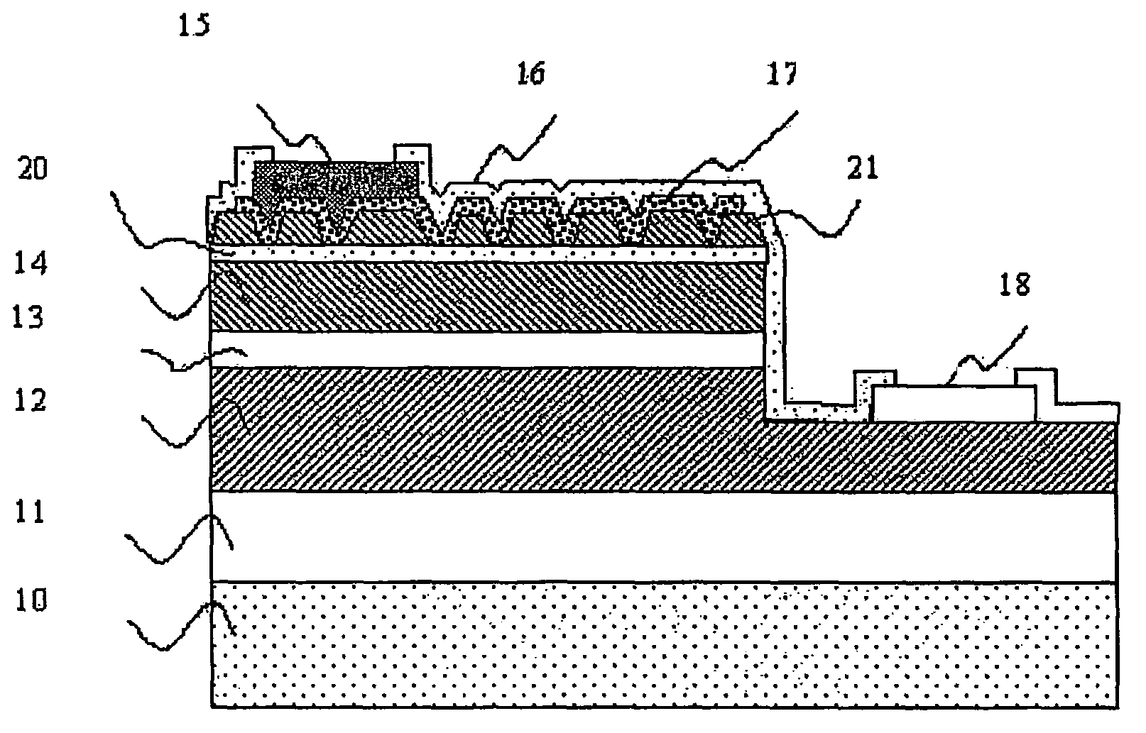
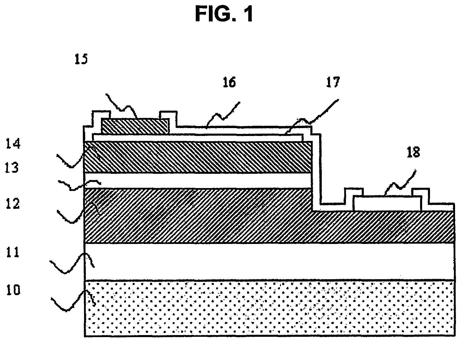
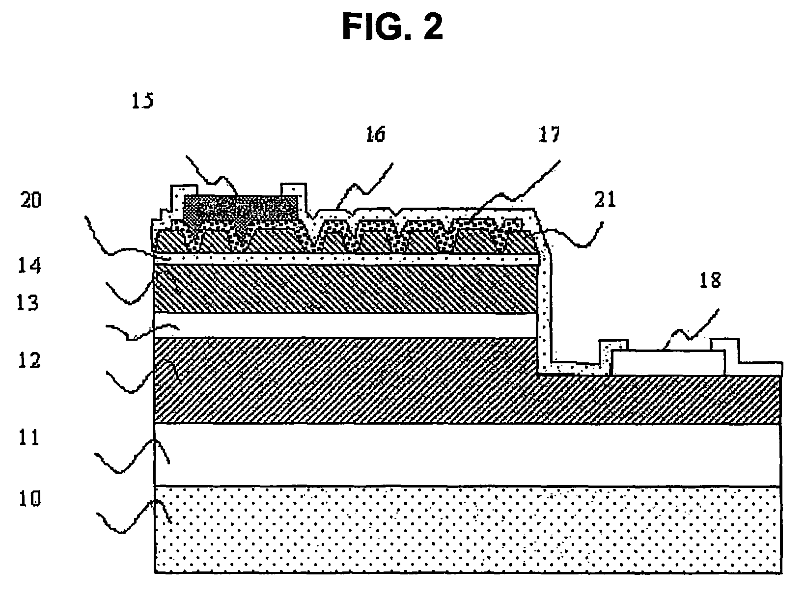
[0055]A III-nitride compound semiconductor light emitting device is fabricated by forming a first layer composed of an n-type silicon carbide (SiaCb), n-type silicon carbon nitride (SicCdNe) or n-type carbon nitride (CfNg) (a, b, c, d, e, f, and g are not 0) layer on a p-type GaN layer forming the existing upper p-side electrode contact layer in a thickness of 5 Å to 1000 Å and growing a second layer composed of a p-type GaN layer on the first layer in a thickness of 100 Å to 5,000 Å.

example 2

[0056]A III-nitride compound semiconductor light emitting device is fabricated by forming a first layer composed of a p-type silicon carbide (SiaCb), p-type silicon carbon nitride (SicCdNe) or p-type carbon nitride (CfNg) (a, b, c, d, e, f, and g are not 0) layer on a p-type GaN layer forming the existing upper p-side electrode contact layer in a thickness of 5 Å to 1000 Å and growing a second layer composed of a p-type GaN layer on the first layer in a thickness of 100 Å to 5,000 Å.

example 3

[0057]A III-nitride compound semiconductor light emitting device is fabricated by forming a first layer composed of an n-type silicon carbide (SiaCb), n-type silicon carbon nitride (SicCdNe) or n-type carbon nitride (CfNg) (a, b, c, d, e, f, and g are not 0) layer on a p-type GaN layer forming the existing upper p-side electrode contact layer in a thickness of 5 Å to 1000 Å and growing a second layer composed of a p-type GaN layer on the first layer in a thickness of 100 Å to 5,000 Å and growing a third layer composed of an n-type GaN layer on the second layer in a thickness of 5 Å to 200 Å. In this case, the third layer is a layer formed using the concept of a tunneling effect.


PUM

PropertyMeasurementUnit
temperatureaaaaaaaaaa

Abstract

The present invention relates a III-nitride compound semiconductor light emitting device in which a first layer composed of a carbon-containing compound layer, such as an n-type or p-type silicon carbide (SiC), silicon carbon nitride (SiCN) or carbon nitride layer (CN) layer, is formed on the p-type III-nitride semiconductor layer of the existing III-nitride semiconductor light emitting device, and a second layer composed of a III-nitride semiconductor layer with a given thickness is formed on the first layer.

Description

CROSS-REFERENCE TO PRIOR APPLICATION[0001]This is a U.S. National Phase Application under 35 U.S.C. §371 of International Patent Application No. PCT / KR2005 / 000895, filed Mar. 25, 2005, which claims priority of Korean Patent Application No. 10-2004-0020270, filed Mar. 25, 2004, both of which are hereby incorporated by reference. The International Application published in English on Jan. 12, 2006 as WO 2006 / 004271 A1 under PCT Article 21(2).TECHNICAL FIELD[0002]The present invention relates to a III-nitride compound semiconductor light emitting device, and more particularly, to a III-nitride compound semiconductor light emitting device with improved external quantum efficiency, which has roughness in a nitride semiconductor layer.[0003]As used herein, the term III-nitride compound semiconductor light emitting device refers to a light emitting device, such as a light emitting diode comprising a compound semiconductor layer made of Al(x)Ga(y)In(1-x-y)N (0≦x≦1, 0≦y≦1, 0≦x+y≦I), and does ...

Claims


Application Information

Patent Timeline
Patent Type & Authority Patents(United States)
IPC IPC(8): H01L33/00H01L21/20H01L21/205H01L21/314H01L21/318H01L33/02H01L33/22H01L33/40
CPCH01L21/02447H01L21/0254H01L21/0262H01L21/3148H01L33/02H01L33/22H01L21/318H01L33/40H01L21/3185H01L21/02167G02C9/02G02C5/2218G02C5/2272G02C2200/02
Inventor YOO, TAE KYUNGPARK, EUN HYUN
Owner EPIVALLEY
Why Eureka
Try Eureka