Digital image processing using white balance and gamma correction

a digital image and white balance technology, applied in the field of digital imaging, can solve the problems of large noise generated by the sensor, large power consumption, and high cost of electronic cooling the sensor with a thermo-electric cooler,

Active Publication Date: 2007-06-26
NXP USA INC
View PDF23 Cites 40 Cited by
  • Summary
  • Abstract
  • Description
  • Claims
  • Application Information

AI Technical Summary

Problems solved by technology

In an image, the resolution is the limit of the ability to depict fine lines, sharp edges, and other details in the original scene.
Unique to digital cameras, a large component of the noise is thermally generated within the sensor.
Cooling the sensor can reduce this noise but electronically cooling the sensor with a Thermo-Electric (TE) cooler is both expensive and consumes quite a bit of power.
CMOS sensors, having many cost, power, and circuit advantages over CCD sensors, tend to have poorer signal-to-noise and dynamic range than CCDs.

Method used


Image

  • Digital image processing using white balance and gamma correction
  • Digital image processing using white balance and gamma correction
  • Digital image processing using white balance and gamma correction

Examples


Embodiment Construction

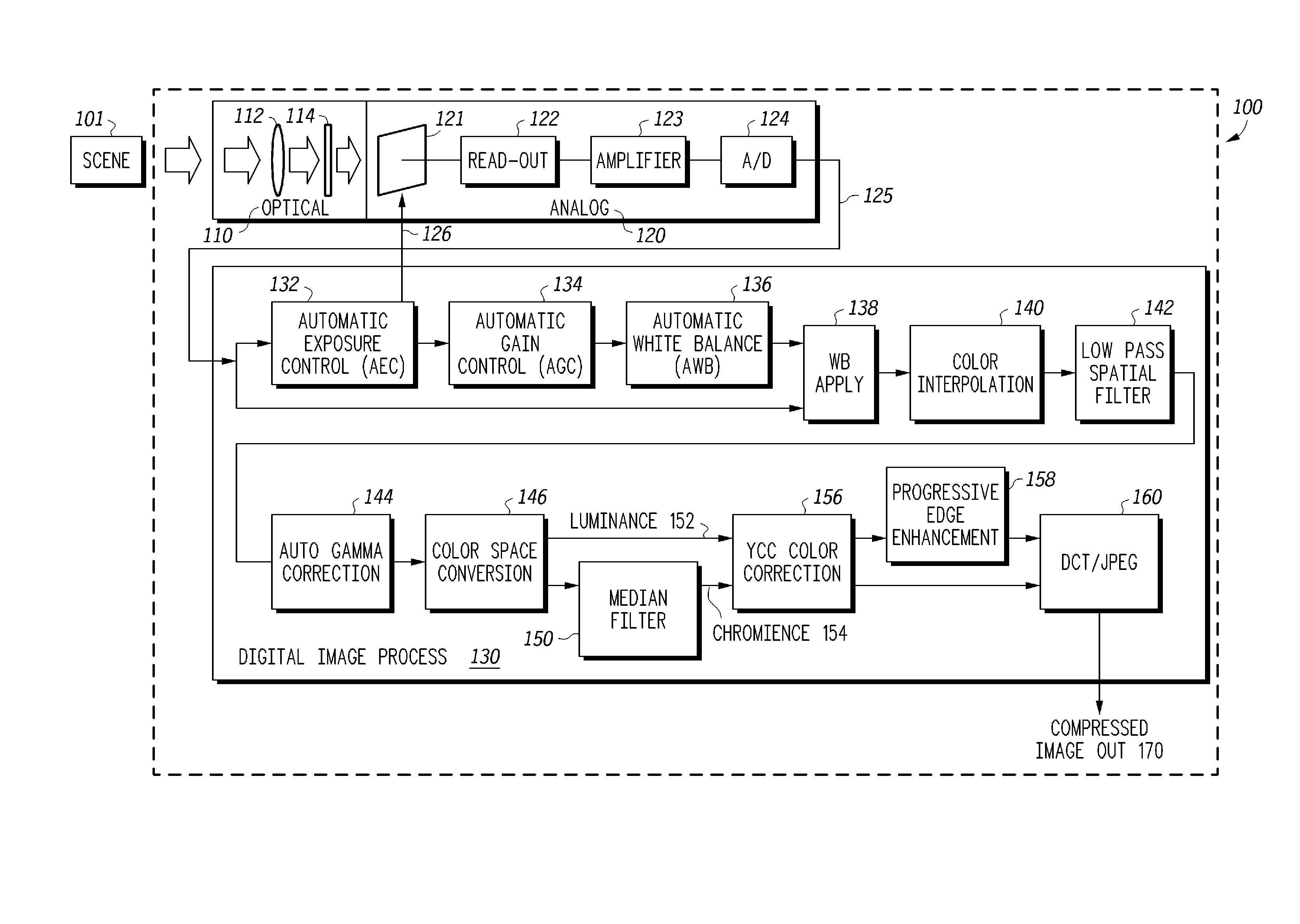
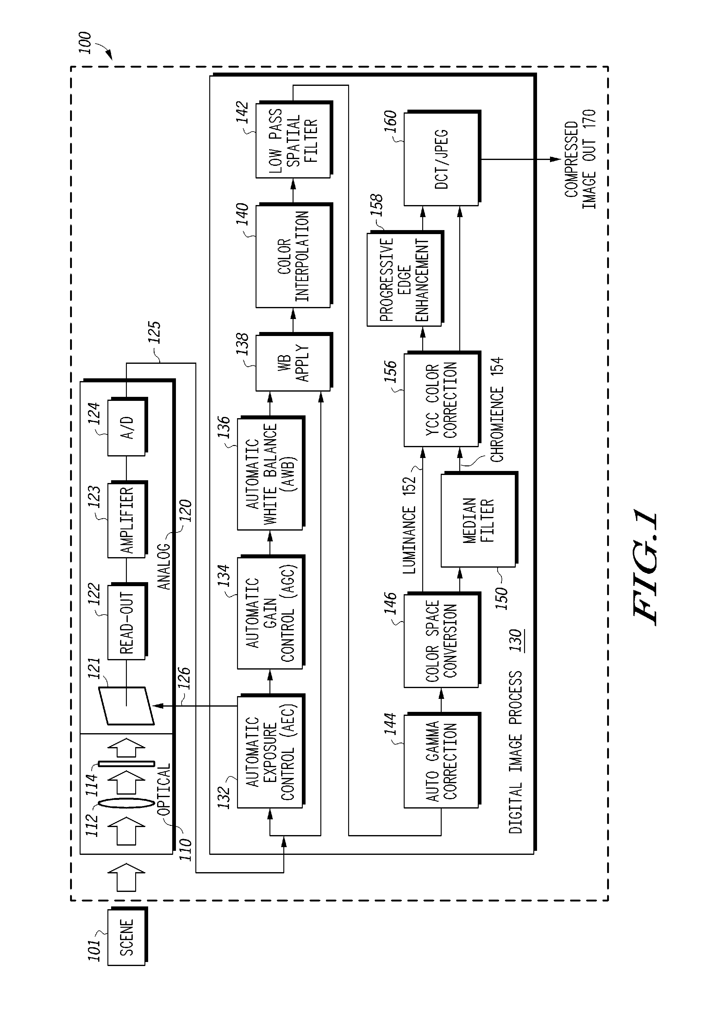
[0023]FIG. 1 shows camera 100 taking a picture of scene 101. Scene 101 may be of people, animals, plants, scenery, buildings, or a mixture thereof. Camera 100 has three major component sections, an optical section 110, an analog section 120, and a digital image process section 130.

[0024]In optical section 110, light from scene 101 is focused by optical lens 112 onto color filter array (CFA) 114. CFA 114 can be a Bayer pattern or another array. The light then enters analog section 120 where it is detected by photo-sensors 121. Photo sensors 121 are a CMOS array. CMOS stands for complementary metal-oxide semiconductor, where pairs of metal-oxide semiconductor field effect transistors (MOSFETs), one N-type and the other P-type, are integrated on a single silicon chip. CMOS devices have high speed and extremely low power consumption. The output of photo-sensors 121 are obtained by read-out 122, amplified by amplifier 123, and then digitized by analog-to-digital (A / D) converter 124.

[0025...


PUM


Abstract

A method and system for digital cameras provides improved automatic exposure control, improved automatic white balance, improved color interpolation, improved automatic gamma correction, and improved progressive edge enhancement. These improvements are preferably implemented in CMOS semiconductor technology for faster speed.

Description

TECHNICAL FIELD OF THE INVENTION[0001]The present invention relates to the field of methods and systems for digital imaging.BACKGROUND OF THE INVENTION[0002]Digital imaging systems have created a revolution in photography and cameras. A digital camera is similar to a film camera except that the film is replaced with an electronic sensor. The sensor is comprised of an array of photo detectors that change the photons that strike them into electrons providing a signal at each pixel proportional to the number of photons, or the amount of light at each pixel. Presently, most consumer digital cameras employ Charge Coupled Device (CCD) or Complementary Metal Oxide Semiconductor (CMOS) sensors. To facilitate the collection of light, many of the sensors employ a small lens-like structure covering each pixel, which is called a microlens. These microlenses are typically made by forming a layer of photoresist that is placed upon the pixel plane.[0003]The image sensors used in digital imaging ar...

Claims


Application Information

Patent Timeline
Patent Type & Authority Patents(United States)
IPC IPC(8): H04N5/228G06K9/40H04N5/208H04N5/335H04N9/68H04N9/73H04N5/351H04N5/374H04N9/04H04N9/07H04N9/64
CPCH04N9/045H04N9/735H04N23/843H04N25/134H04N23/88
Inventor YANOF, ARNOLDSKOW, MICHAELTRAN, HUNGADBY, ANOOSH
Owner NXP USA INC
Why Eureka
Try Eureka