Organic field effect transistor with a photostructured gate dielectric, method for the production and use thereof in organic electronics

a photostructured gate dielectric and organic electronics technology, applied in transistors, thermoelectric devices, solid-state devices, etc., can solve the problems of inability to manufacture complex circuits, and inability to meet the requirements of high-temperature electronics

Inactive Publication Date: 2007-07-03
POLYIC GMBH & CO KG
View PDF222 Cites 17 Cited by
  • Summary
  • Abstract
  • Description
  • Claims
  • Application Information

AI Technical Summary

Benefits of technology

[0009]The object of the present invention was therefore to specify an organic field effect transistor or a method for the manufacture thereof which permits the use of photolithography without attacking or dissolving the organic layers in all operations as well as making possible a construction which provides a simple means of vertical interconnection between conducting tracks at different levels in organic integrated circuits. The organic field effect transistors must at the same time be manufacturable cheaply and economically using simple operations.

Problems solved by technology

This is possible only to a very limited extent using conventional photolithography which is actually used for patterning inorganic materials.
The operations normally involved in photolithography dissolve or attack the organic layers and therefore make them unusable.
However, it has been shown that in particular the last operation for forming the vertical interconnects (otherwise known as vias) does not permit the fabrication of complex circuits.
If a “top gate” structure of the same composition were produced, this would result in unacceptable contact resistances in the order of M.
However, the construction and the operations for patterning this OFET with bottom gate structure are complex, making it impossible to manufacture particularly complex circuits economically.

Method used


Image

  • Organic field effect transistor with a photostructured gate dielectric, method for the production and use thereof in organic electronics
  • Organic field effect transistor with a photostructured gate dielectric, method for the production and use thereof in organic electronics
  • Organic field effect transistor with a photostructured gate dielectric, method for the production and use thereof in organic electronics

Examples


Embodiment Construction

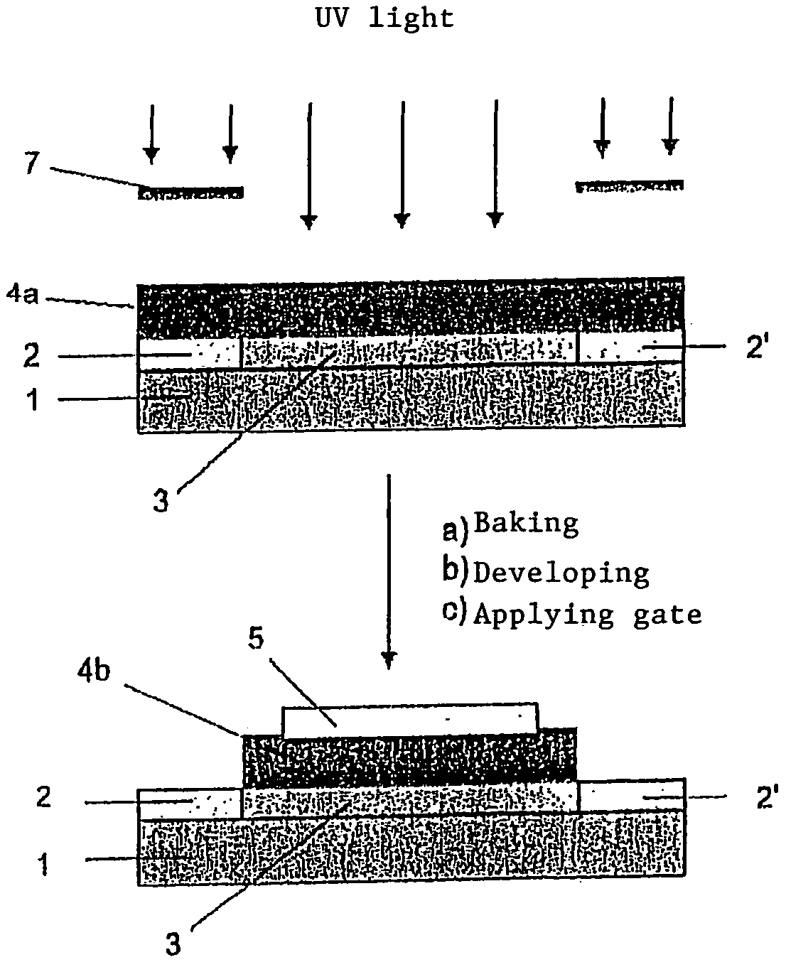
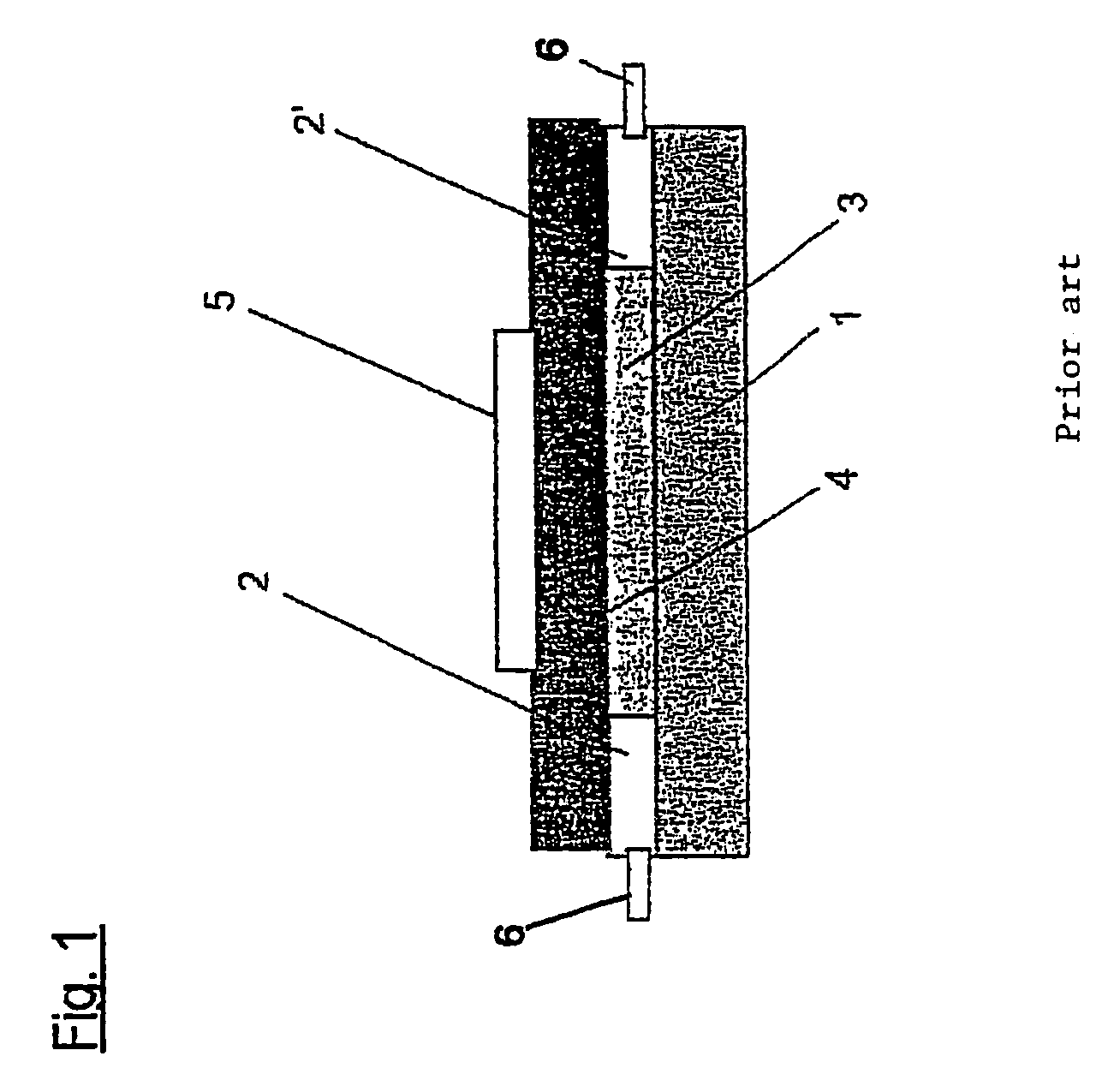
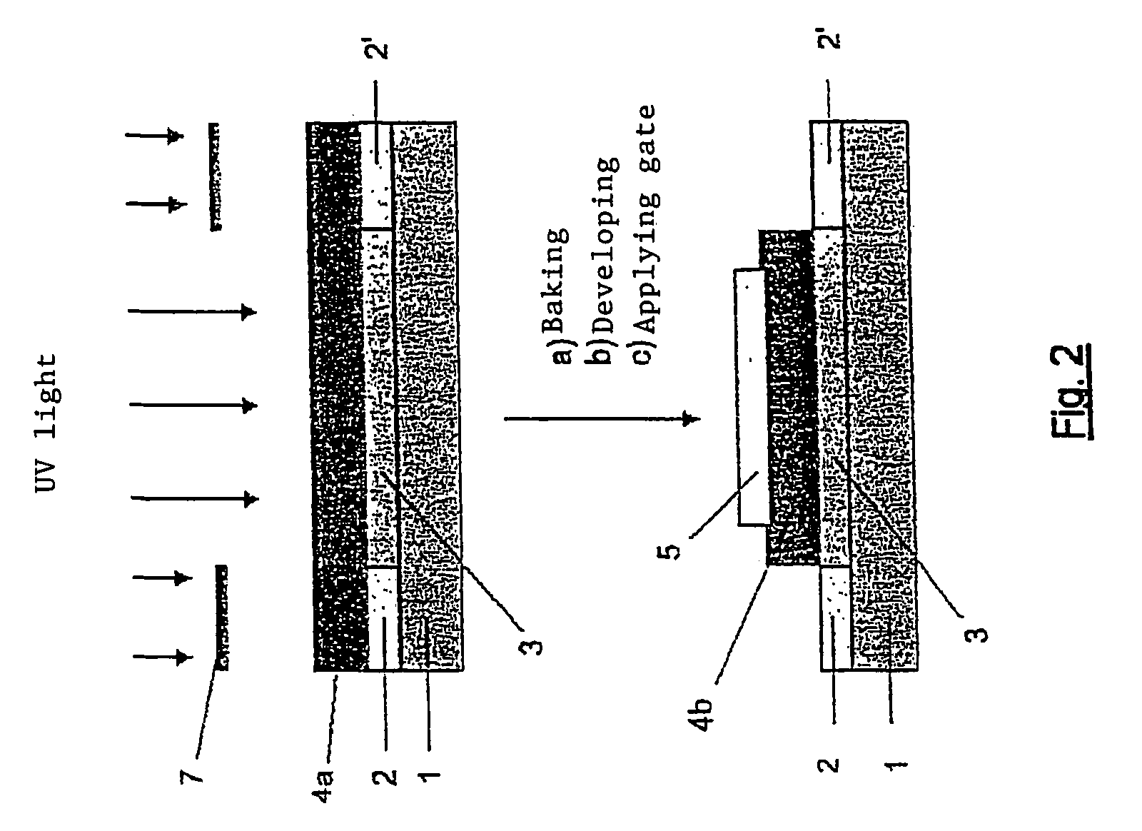
[0023]A conventional OFET consists of a substrate 1, source and drain electrodes 2 and 2′, a semiconductor 3, an insulator 4 and the gate electrode 5. The conventional OFET requires contact tags 6 for combining individual OFETs to form larger circuits.

[0024]As shown in FIG. 2, the starting point for producing an OFET according to the invention is a similar structure to that of a conventional OFET. In other words, on a substrate 1 there are formed source and drain electrodes 2 and 2′ as well as a semiconductor layer 3. The source and drain electrodes 2 and 2′ as well as the semiconductor 3 are in one layer. On this layer a thin layer of an insulator material such as poly(4-hydroxystyrene) (PVP) or melamine-formaldehyde resins containing hydroxyl groups is deposited by spin-coating, screen printing or similar processes. The solution to be applied contains, in addition to the insulator material, an acid-sensitive crosslinker such as hexamethoxymethylmelamine (HMMM) and a photoinitiator...


PUM

PropertyMeasurementUnit
temperatureaaaaaaaaaa

Abstract

The invention relates to an organic field effect transistor which is especially characterized by a cross-linked, structured insulating layer (4) on which the gate electrode (5) is arranged. The structure of the OFET ensures that the gate electrode (5) of an OFET can be used as a strip conductor to the source electrode (2) of the next transistor and can be used in the construction of larger circuits.

Description

CROSS REFERENCE TO RELATED APPLICATIONS[0001]This is the 35 USC 371 national stage of international application PCT / DE02 / 00312 filed on Jan. 29, 2002, which designated the United States of AmericaFIELD OF THE INVENTION[0002]The present invention relates to organic field effect transistors, so-called OFETs, with photopatterned gate dielectric as well as a method for the production thereof, and the use of said field effect transistors in organic electronics.BACKGROUND OF THE INVENTION[0003]Field effect transistors play a central role in all areas of electronics. In order to adapt them to suit particular applications, it has been necessary to make them lighter and more flexible. The development of semiconducting and conducting polymers has made it possible to produce organic field effect transistors, all parts of which, including the semiconductor layer as well as the source, drain and gate electrodes, are fabricated from polymeric materials.[0004]However, in the production of organic ...

Claims


Application Information

Patent Timeline
Patent Type & Authority Patents(United States)
IPC IPC(8): H01L35/24H01L21/31H01L29/76H01L29/94H01L51/00H01L51/05H01L21/336H01L27/28H01L29/786H01L51/30H01L51/40
CPCH01L51/0516H01L27/28H01L51/0015H01L51/0021H01L51/0035H01L51/0037H01L51/0097H01L51/0541H10K71/211H10K71/60H10K85/111H10K85/1135H10K10/468H10K10/464H10K77/111H10K19/80H10K19/00
Inventor BERNDS, ADOLFFIX, WALTERROST, HENNING
Owner POLYIC GMBH & CO KG
Why Eureka
Try Eureka