Arbitration of data transfer requests

a data transfer request and data technology, applied in the field of data processing systems, can solve problems such as particularly acute problems, and achieve the effect of accelerating the transfer

Active Publication Date: 2007-07-03
ARM LTD
View PDF7 Cites 5 Cited by
  • Summary
  • Abstract
  • Description
  • Claims
  • Application Information

AI Technical Summary

Benefits of technology

[0007]The present invention recognises that in some circumstances it is particularly important that data can be transferred quickly to or from a particular memory. It addresses this problem by providing a memory access interface. The division of the core into portions has several advantages, one is that data may be transferred faster than would be the case if the data was transferred via a standard processor core as the instructions required to read the data, store it in a register on the core and then write it to a memory are not required. However, a problem associated with providing a memory access interface portion of the core along side the processing portion is that both portions may wish to access data stored in an associated memory at the same time. This problem can be particularly acute in applications such as data logging, where a large amount of data that does not need to be processed immediately is transferred via the core to a memory.
[0008]This problem is addressed by providing at least two buses operable to provide data communication between the processor core and the associated memory, the associated memory being divided into at least two portions, a bus providing data access to respective portions. Arbitration logic is provided in association with the bus and the read / write port and is operable to route data access requests requesting access to data in a particular portion of the memory to the appropriate bus. The provision of more than one bus allows data access requests to different portions of the memory that are received from the memory access interface and the data processing portion of the core in the same clock cycle to be processed in parallel along respective buses. This alleviates some of the problems that can occur when two portions of the core are trying to access one memory via a single bus.
[0014]By dividing the data portions into odd and even address portions, a data access request that accesses a large number of concurrently stored data items will use alternate data buses. This means that it is highly unlikely that one of the portions of the processor core will monopolise one of the data buses for a long period and thereby prevent access to the corresponding portion of the memory by the other portion of the processor core.
[0016]The arbitration logic is operable to give priority to the memory access interface when data access requests from both portions are received during the same processor clock cycle. This is because the memory access interface is provided on the processor core in order to give fast access to memory and thus it makes sense to give it priority. The provision of a plurality of buses helps prevent the processing portion of the core being denied access to a memory over a long period of time which could seriously affect operation of the core particularly if important code is being executed by the processing portion of the core.
[0018]In some embodiments the memory may not operate as fast as the processor clock. In such cases, it is highly convenient that a wait signal can be used which the arbitration logic understands. This prevents data access requests being sent to or from the memory faster than it can cope with them.

Problems solved by technology

However, a problem associated with providing a memory access interface portion of the core along side the processing portion is that both portions may wish to access data stored in an associated memory at the same time.
This problem can be particularly acute in applications such as data logging, where a large amount of data that does not need to be processed immediately is transferred via the core to a memory.

Method used


Image

  • Arbitration of data transfer requests
  • Arbitration of data transfer requests
  • Arbitration of data transfer requests

Examples


Embodiment Construction

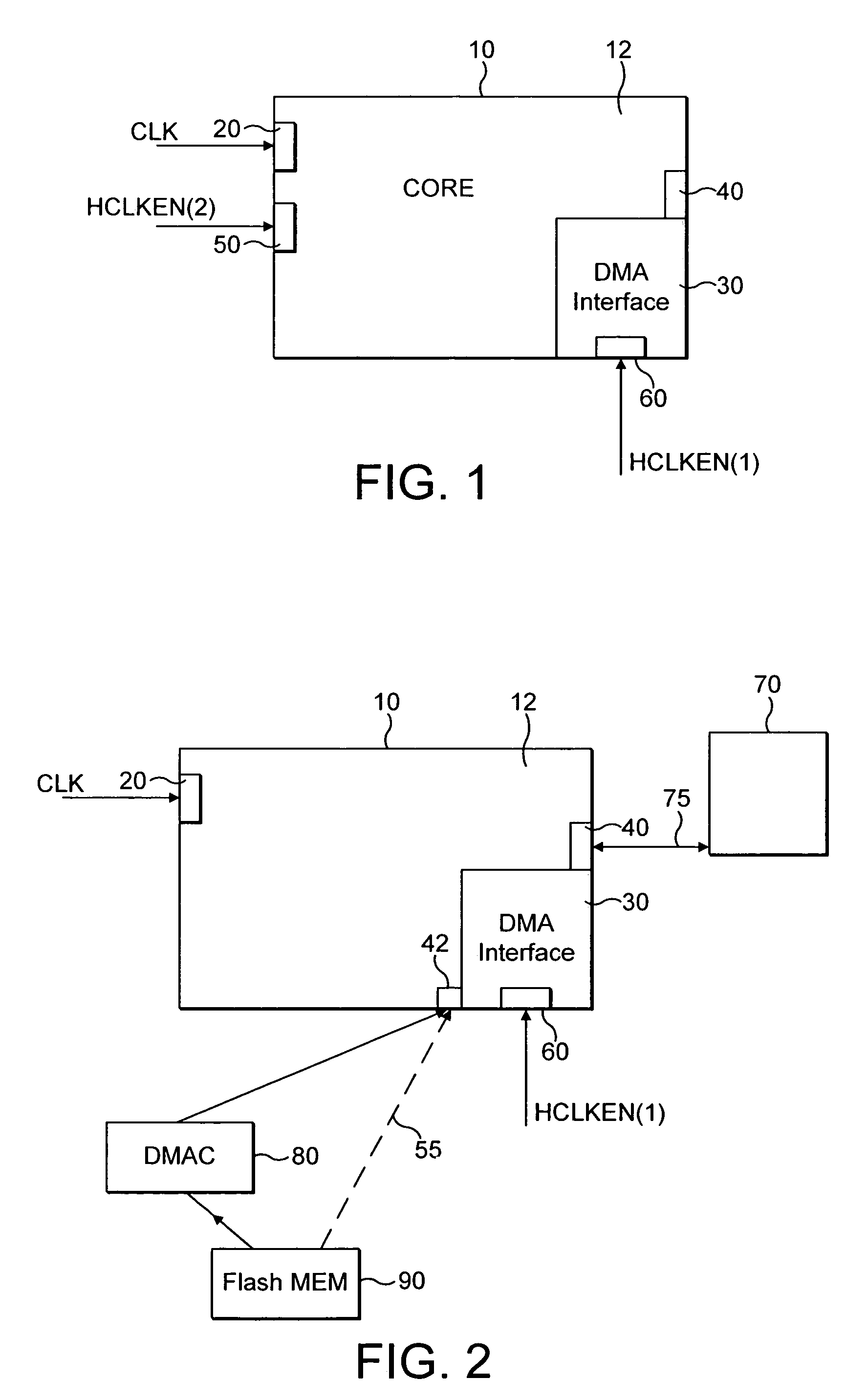
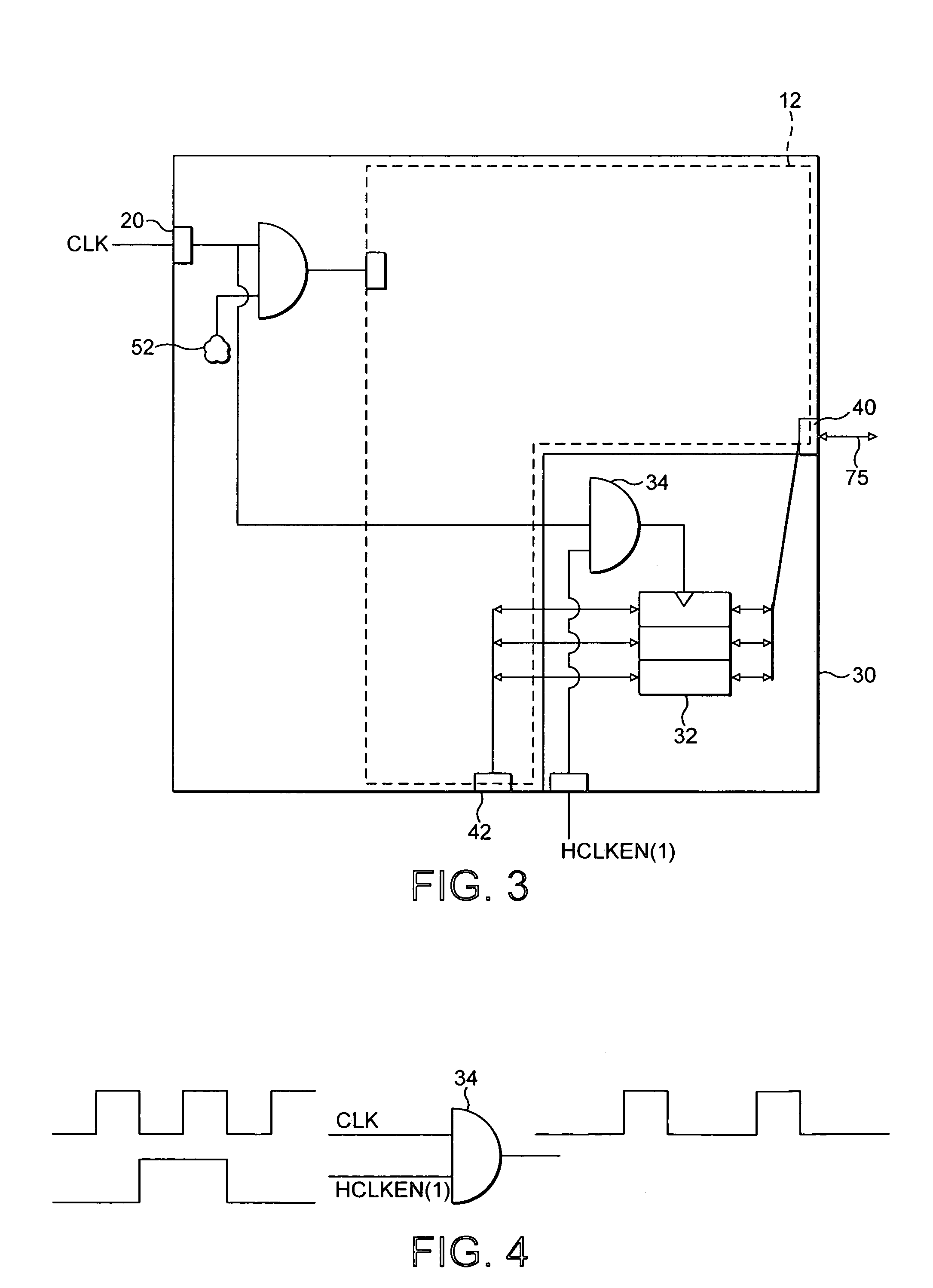
[0032]FIG. 1 shows a processor core 10 which is divided into portions, one portion 12 being a standard data processing portion, and the other portion being a direct memory interface (DMA) 30. The processor core 10 has a clock signal input 20 for receiving a processor clocking signal CLK, and at least one read / write port 40 operable to be connected via a bus to memory associated with the core. The core may also have two further inputs a memory access enable signal input 60 for receiving a clock enable signal HCLKEN(1) and a processor enable input 50 for receiving a clock enable signal HCLKEN(2). In some embodiments the processor enable signal HCLKEN(2) is not received as an external signal, but is generated by processing logic within the core (see FIG. 3). The processing portion 12 of the core is clocked by the processor clock signal CLK when the HCLKEN(2) signal has a predetermined value in this embodiment when it is 1. When the HCLKEN(2) signal is 0 the processing portion does not ...


PUM


Abstract

A data processor core 10 comprising: a memory access interface portion 30 operable to perform data transfer operations between an external data source and at least one memory 120 associated with said data processor core; a data processing portion 12 operable to perform data processing operations; a read / write port 40 operable to transfer data from said processor core to at least two buses 75A, 75B said at least two buses being operable to provide data communication between said processor core 10 and said at least one memory 120, said at least one memory 120 comprising at least two portions 120A, 120B, each of said at least two buses 75A, 75B being operable to provide data access to respective ones of said at least two portions 120A, 120B; arbitration logic 110 associated with said read / write port 40; wherein said arbitration logic is operable to route a data access request requesting access of data in one portion of said at least one memory received from said memory access interface to one of said at least two buses providing access to said one portion of said at least one memory and to route a further data access request requesting access of data in a further portion of said at least one memory received from said data processing portion to a further one of said at least two buses providing access to said further portion of said at least one memory, said routing of said data access requests being performed during the same clock cycle.

Description

BACKGROUND OF THE INVENTION[0001]1. Field of the Invention[0002]This invention relates to the field of data processing systems. More particularly, this invention relates to the field of data transfer requests.[0003]2. Description of the Prior Art[0004]In data processing systems it is often necessary to transfer data from one memory to another, or between an external data source and a memory associated with the data processor. For example, in boot up codes may be stored in a slow memory such as a Flash and prior to them being used, it may be desirable to transfer them to a faster instruction memory associated with the processor. Generally, such transfers occurs via the data processor core, with a load instruction specifying a location in the Flash memory from which the data is to be read and a register in the core to which the data item is to be written, and a store instruction specifying the register in the core and the destination location in the faster instruction memory. Such a t...

Claims


Application Information

Patent Timeline
Patent Type & Authority Patents(United States)
IPC IPC(8): G06F12/00G06F13/16G06F12/06G06F13/28G06F13/36
CPCG06F13/1657G06F13/28G06F13/1605
Inventor TRAN, TAN BAWILLIAMS, GERARD RICHARDMATHENY, DAVID TERRENCEFLYNN, DAVID WALTER
Owner ARM LTD
Why Eureka
Try Eureka