Method of manufacturing a polysilicon layer and a mask used therein

a polysilicon and manufacturing method technology, applied in the field of manufacturing a polysilicon layer, can solve the problems of poor utilization rate of laser beam, additional manufacturing steps and manufacturing costs, etc., and achieve the effects of prolonging the melting time of silicon, reducing the usage of laser beam, and prolonging the maintenance period of laser beam optical modules

Active Publication Date: 2007-07-10
AU OPTRONICS CORP
View PDF14 Cites 3 Cited by
  • Summary
  • Abstract
  • Description
  • Claims
  • Application Information

AI Technical Summary

Benefits of technology

[0008]It is therefore an object of the invention to provide a method of manufacturing a polysilicon layer and a mask used in the method. The design of having a semi-transparent region disposed on the mask for the amorphous silicon layer to be preheated has the advantages of enabling the amorphous silicon to reach melting point earlier, reducing the usage of laser beam, and prolonging the lifespan and the maintenance period of the laser beam optical module. Besides, the present embodiment can prolong silicon melting time and increase the distance of lateral crystallization and the manufacturing range of crystallization. Besides, the present embodiment can repair the defects on the polysilicon layer and increase the utilization rate of the laser beam.

Problems solved by technology

Although the defects 13a can be repaired by using the laser beam 16 again or using high-temperature treatment, additional manufacturing steps and manufacturing costs would occur.
Besides, only part of the laser beam 16 would penetrate through the transparent region 15c and melt part of the amorphous silicon layer 12, so another part of the laser beam 16 would be partly reflected and absorbed by the non-transparent region 15a and converted into heat, resulting in a poor utilization rate of the laser beam 16.

Method used


Image

  • Method of manufacturing a polysilicon layer and a mask used therein
  • Method of manufacturing a polysilicon layer and a mask used therein
  • Method of manufacturing a polysilicon layer and a mask used therein

Examples


first embodiment

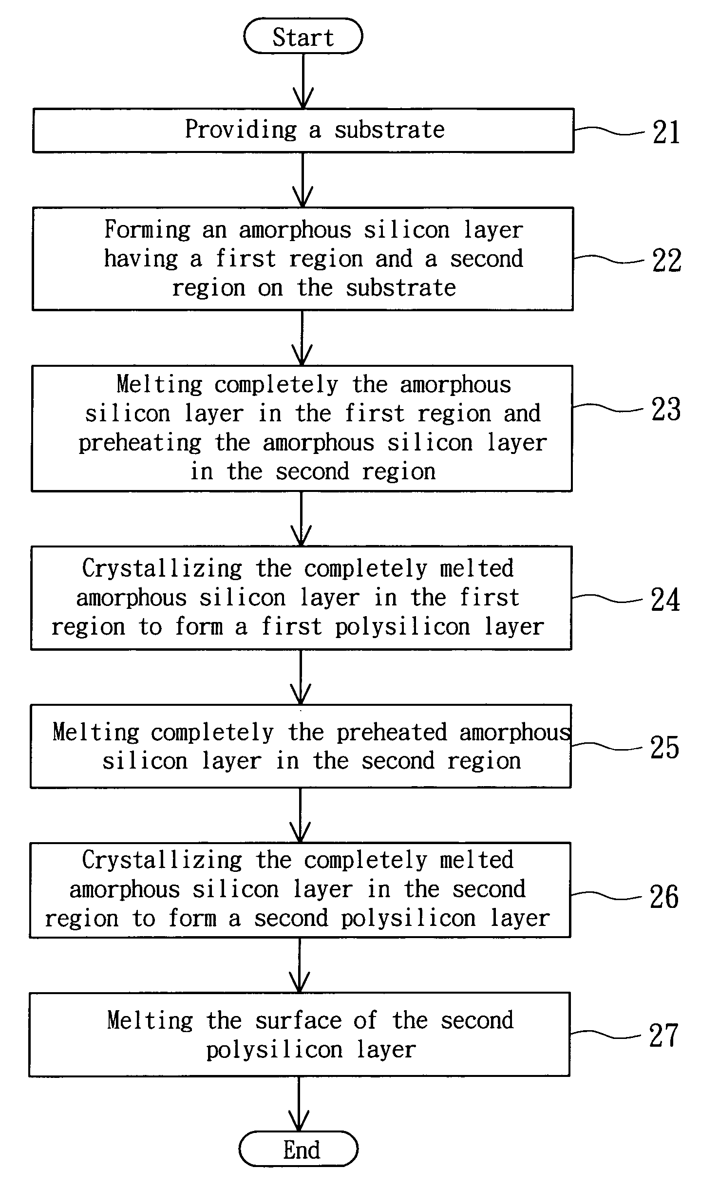
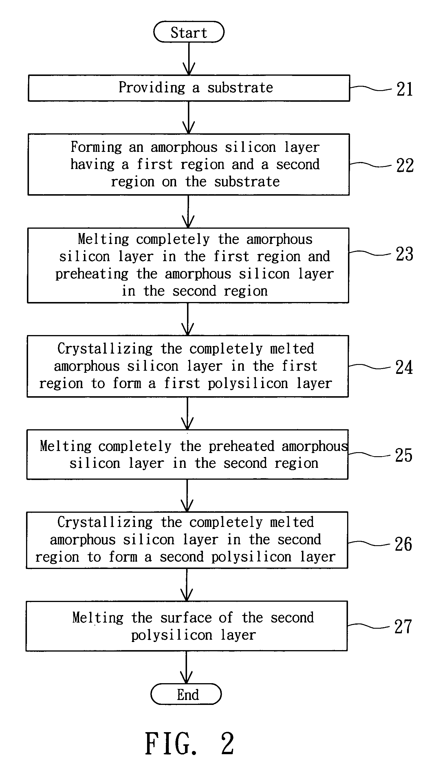
[0017]Referring to FIGS. 2 and 3A˜3E, wherein FIG. 2 is a flowchart diagram of a method of manufacturing a polysilicon layer according to a first embodiment of the invention, while FIGS. 3A˜3E are flowchart diagrams of a method of manufacturing a polysilicon layer according to a first embodiment of the invention. Firstly, the method begins at step 21: a substrate 21 is provided as shown in FIG. 3A. Next, proceed to the step 22 of FIG. 2: an amorphous silicon layer 32 having a first region 32a and a second region 32b is formed on the substrate 31 as shown in FIG. 3B. After that, proceed to step 23: the amorphous silicon layer 32 in the first region 32a is completely melted and the amorphous silicon layer 32 in the second region 32b is preheated as shown in FIG. 3C. Then, proceed to step 24: the completely melted amorphous silicon layer in first region 32a is crystallized to form a first polysilicon layer 33a as shown in FIG. 3D.

[0018]To achieve the object of completely melting the am...

second embodiment

[0024]Referring to FIG. 5, a top view of a mask for the laser beam to preheat and melt an amorphous silicon layer according to a second embodiment of the invention is shown. In FIG. 5, a mask 55 is used for a laser beam to preheat and melt an amorphous silicon layer disposed on a substrate. The amorphous silicon layer has a first region and a second region, while the mask 55 is moved relatively to the substrate. The technology of forming an amorphous silicon layer on the substrate and moving a mask relatively to the substrate are disclosed in the first embodiment and is not repeated in the present embodiment again. The mask 55 comprises a mask body 55b, a non-transparent region 55a, a first mask pattern 56, a second mask pattern 57 and a semi-transparent region 55d. The non-transparent region 55a is formed on the mask body 55b. The first mask pattern 56, the second mask pattern 57 and the semi-transparent region 55d are mutually separated and formed on the mask body 55b. The second ...


PUM

PropertyMeasurementUnit
thicknessaaaaaaaaaa
semi-transparentaaaaaaaaaa
transparentaaaaaaaaaa

Abstract

A method of manufacturing a polysilicon layer is provided. Firstly, a substrate is provided. Next, an amorphous silicon having a first region and a second region is formed on the substrate. After that, the amorphous silicon layer in the first region is completely melted and the amorphous silicon layer in the second region is preheated. The completely melted amorphous silicon layer in the first region is crystallized to form a first polysilicon layer. Next, the preheated amorphous silicon layer in the second region is completely melted. The completely melted amorphous silicon layer in the second region is crystallized to form a second polysilicon layer.

Description

[0001]This application claims the benefit of Taiwan application Serial No. 93134997, filed Nov. 15, 2004, the subject matter of which is incorporated herein by reference.BACKGROUND OF THE INVENTION[0002]1. Field of the Invention[0003]The invention relates in general to a method of manufacturing a polysilicon layer, and more particularly to a method of manufacturing a polysilicon layer using a mask for the laser beam to preheat an amorphous silicon layer and completely melt the preheated amorphous silicon layer, and the mask therein.[0004]2. Description of the Related Art[0005]With the rapid development in science and technology, display panel has been widely used in electronic devices such as notebook, personal digital assistant (PDA) and mobile phone. The display panel has two categories, namely, the amorphous silicon (a-Si) thin film transistor (TFT) display panel and the low temperature polysilicon (LTPS) TFT display panel. The main difference between the LTPS TFT display panel a...

Claims


Application Information

Patent Timeline
Patent Type & Authority Patents(United States)
IPC IPC(8): H01L21/20
CPCB23K26/0656C30B13/00C30B29/06G03F1/14G03F1/144H01L21/2026B23K26/066H01L21/02532H01L21/02691H01L21/0268H01L21/02595
Inventor SUN, MING-WEI
Owner AU OPTRONICS CORP
Why Eureka
Try Eureka