Method to form relaxed SiGe layer with high Ge content using co-implantation of silicon with boron or helium and hydrogen

a technology of boron or helium and high ge content, applied in the direction of basic electric elements, electrical apparatus, semiconductor devices, etc., can solve the problems of insufficient thickness of 2000 –2500 for device application, inability to integrate several m sisub>1-x/sub>ge/sub>x into device fabrication, etc., to achieve the effect of improving film properties and low cos

Inactive Publication Date: 2007-07-10
SHARP KK
View PDF11 Cites 5 Cited by
  • Summary
  • Abstract
  • Description
  • Claims
  • Application Information

AI Technical Summary

Benefits of technology

[0012]Another object of the invention is to provide a method of fabricating such a film which is low in cost and which has improved film properties.

Problems solved by technology

In addition, the integration of several μm Si1-xGex into device fabrication is not practical.
SiGe having a 2000 Å–2500 Å thickness is not sufficient for device application.

Method used


Image

  • Method to form relaxed SiGe layer with high Ge content using co-implantation of silicon with boron or helium and hydrogen
  • Method to form relaxed SiGe layer with high Ge content using co-implantation of silicon with boron or helium and hydrogen
  • Method to form relaxed SiGe layer with high Ge content using co-implantation of silicon with boron or helium and hydrogen

Examples


Embodiment Construction

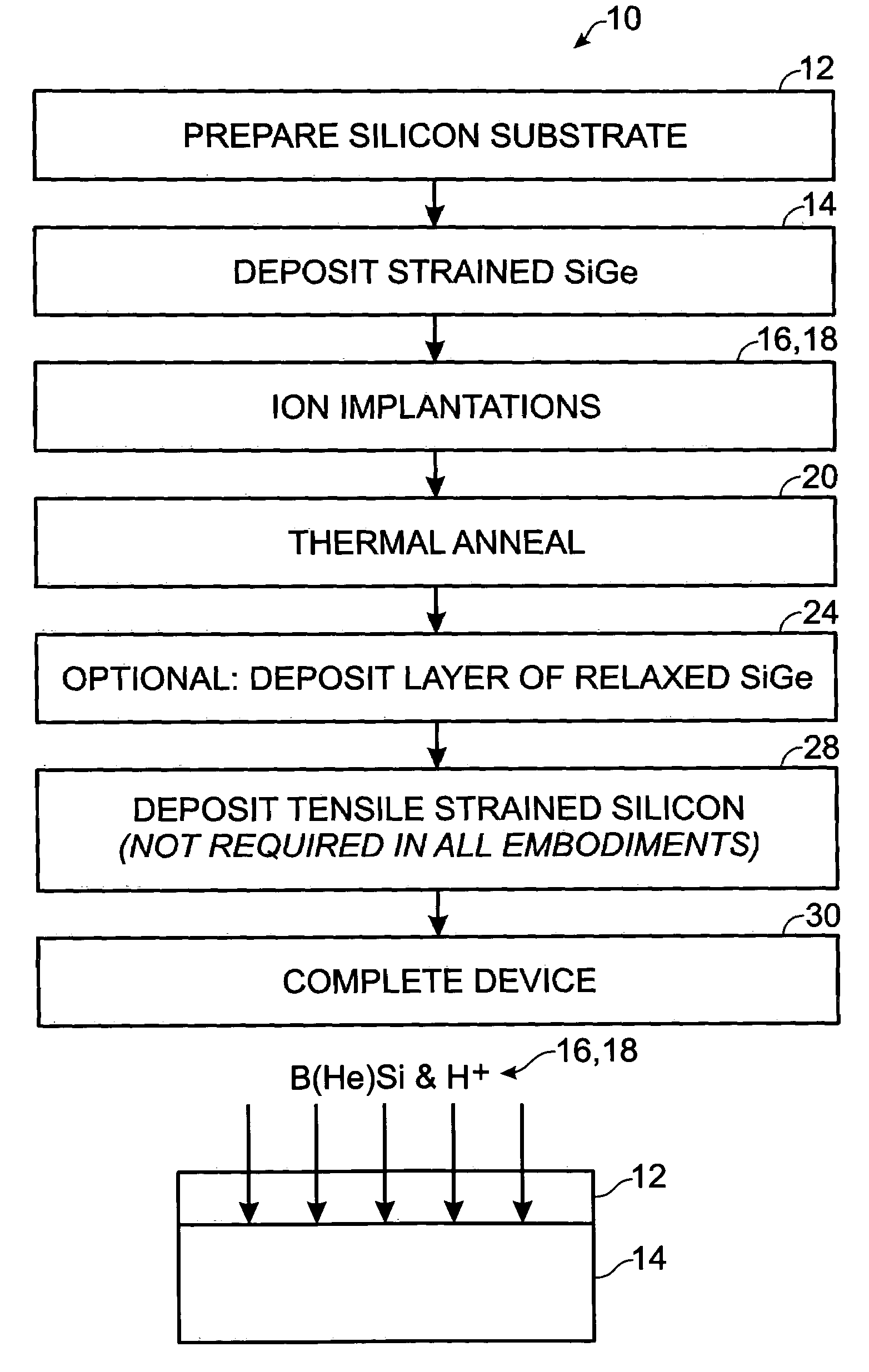
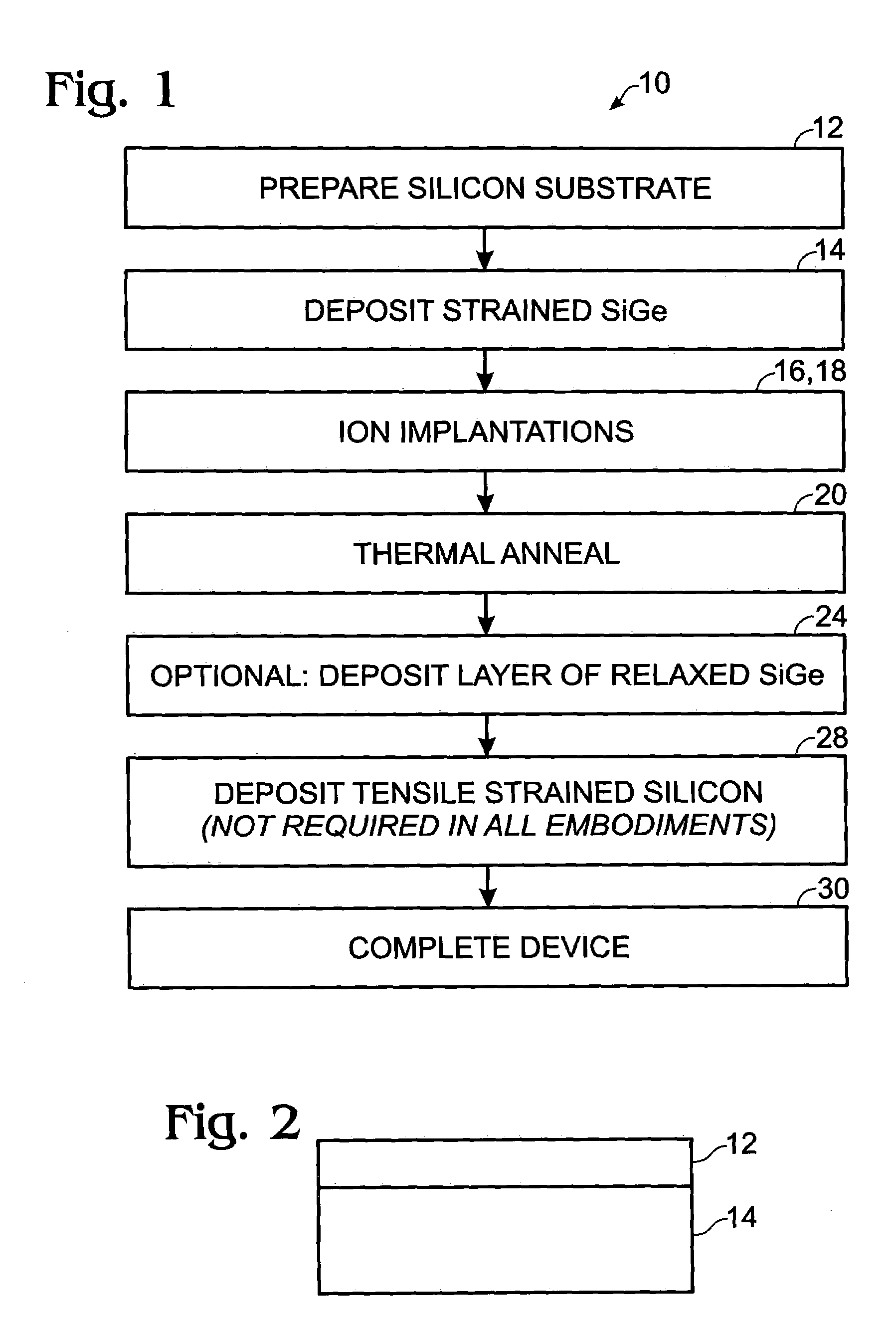
[0017]The method of the invention results in a thick, e.g., 100 nm to 500 nm, relaxed, smooth SiGe film having a high germanium content, e.g., >20% to 30% or more, for use as a buffer layer for a tensile strained silicon film, all of which are used in high-speed MOSFET applications. Our previous work, and that of others, has demonstrated that hydrogen implantation is effective for producing such films. However, now-conventional hydrogen implantation is both costly and requires time-consuming post-implantation steps. The purpose of the present invention is to reduce the hydrogen implantation dose and / or the annealing temperature and time to both reduce cost and improve the final film properties.

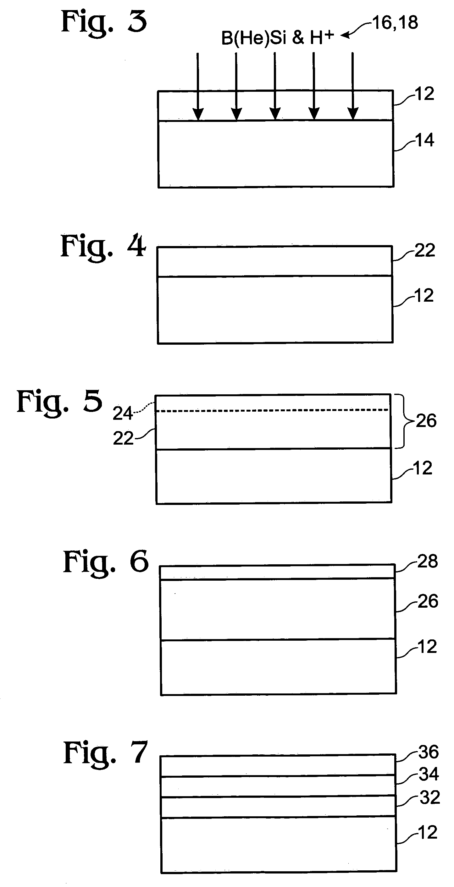
[0018]The method of the invention is depicted generally in FIG. 1 at 10, and is shown in sequential steps depicted in FIGS. 2–6. Referring now to FIGS. 1 and 2, a silicon substrate is prepared 12, and a layer of strained SiGe 14, having a thickness of between about 100 nm to 500 nm, is deposit...


PUM

PropertyMeasurementUnit
temperatureaaaaaaaaaa
thicknessaaaaaaaaaa

Abstract

A method of forming a relaxed SiGe layer having a high germanium content in a semiconductor device includes preparing a silicon substrate; depositing a strained SiGe layer; implanting ions into the strained SiGe layer, wherein the ions include silicon ions and ions selected from the group of ions consisting of boron and helium, and which further includes implanting H+ ions; annealing to relax the strained SiGe layer, thereby forming a first relaxed SiGe layer; and completing the semiconductor device.

Description

FIELD OF THE INVENTION[0001]This invention relates to high speed CMOS integrated circuit, and specifically to fabrication of such a device having a relaxed SiGe layer therein.BACKGROUND OF THE INVENTION[0002]In enhanced mobility MOSFET device applications thick, relaxed Si1-xGex, buffer layers have been used as virtual substrates for thin, strained silicon layers to increase carrier mobility for both NMOS Welser et al., Electron mobility enhancement in strained-Si N-type metal-oxide-semiconductor transistors, 1994 IEDM Conference Proceedings, p. 373 (1994).IEEE EDL-15, #3, p. 100, (1994); Rim et al., (Rim I) Fabrication and analysis of Deep submicron strained-Si N-MOSFETs, IEEE Transactions on Electron Devices, Vol 47, 1406, (2000); and Rim et al., (Rim II) Strained Si NMOSFETs for High Performance CMOS Technology, 2001 Symposium on VLSI Technology Digest of Technical Papers, p. 59, IEEE 2001; and PMOS, Rim et al., (Rim III) Enhanced hole mobilities in surface-channel strained-Si p-...

Claims


Application Information

Patent Timeline
Patent Type & Authority Patents(United States)
IPC IPC(8): H01L21/26H01L21/42
CPCH01L21/02381H01L21/0245H01L21/02532H01L21/02694H01L29/1054Y10S438/933
Inventor TWEET, DOUGLAS J.EVANS, DAVID R.HSU, SHENG TENGMAA, JER-SHEN
Owner SHARP KK
Why Eureka
Try Eureka