Method and apparatus for minimizing phase error and jitter in a phase-locked loop

a phase-locked loop and phase error technology, applied in the direction of automatic control of pulses, process and machine control, etc., can solve the problems of reducing the tolerance for clock jitter and phase error, undesired phase error and jitter at the clock output, and increasing the difficulty of pll design, so as to minimize phase error and jitter, and minimize charge build-up

Active Publication Date: 2007-07-10
ORACLE INT CORP
View PDF6 Cites 6 Cited by
  • Summary
  • Abstract
  • Description
  • Claims
  • Application Information

AI Technical Summary

Benefits of technology

[0012]One embodiment of the present invention provides an apparatus that minimizes phase error and jitter in a phase-locked loop. The apparatus includes a phase / frequency detector, a charge pump, a loop filter, a voltage-controlled oscillator, and a frequency divider, which are coupled together to form a phase-locked loop. The charge pump within the phase-locked loop contains a pull-up network and a pull-down network which are coupled to each other, and a current compensation device. If the pull-up network and the pull-down network are both conducting, the current compensation device adjusts currents flowing through the pull-up network and through the pull-down network such that the currents are substantially equal. This ensures that very little current flows into the loop filter, thereby substantially minimizing a build-up of charge on a capacitor in the loop filter, which can cause phase error and jitter in the phase-locked loop.

Problems solved by technology

Unfortunately, PLL design is becoming more difficult.
Furthermore, modern high-performance systems are using high frequency clock signals in the multi-GHz range; these high frequencies reduce the tolerance for clock jitter and phase error.
This build-up, in turn, causes a shift in frequency and results in undesired phase error and jitter at the clock output.
Because an ideal charge pump is not feasible using existing technologies, the most common solution to mitigate the current mismatch problem is to cascode the current sources to boost the output impedances.
However, boosting the output impedances reduces the output voltage swing of the charge pump.
Furthermore, with sub-one-Volt power supplies, cascoding is no longer feasible because it reduces the voltage headroom for the transistors in the pull-up network and the pull-down network.
This ensures that very little current flows into the loop filter, thereby substantially minimizing a build-up of charge on a capacitor in the loop filter, which can cause phase error and jitter in the phase-locked loop.

Method used


Image

  • Method and apparatus for minimizing phase error and jitter in a phase-locked loop
  • Method and apparatus for minimizing phase error and jitter in a phase-locked loop
  • Method and apparatus for minimizing phase error and jitter in a phase-locked loop

Examples


Embodiment Construction

[0030]The following description is presented to enable any person skilled in the art to make and use the invention, and is provided in the context of a particular application and its requirements. Various modifications to the disclosed embodiments will be readily apparent to those skilled in the art, and the general principles defined herein may be applied to other embodiments and applications without departing from the spirit and scope of the present invention. Thus, the present invention is not limited to the embodiments shown, but is to be accorded the widest scope consistent with the principles and features disclosed herein.

Charge Pump System

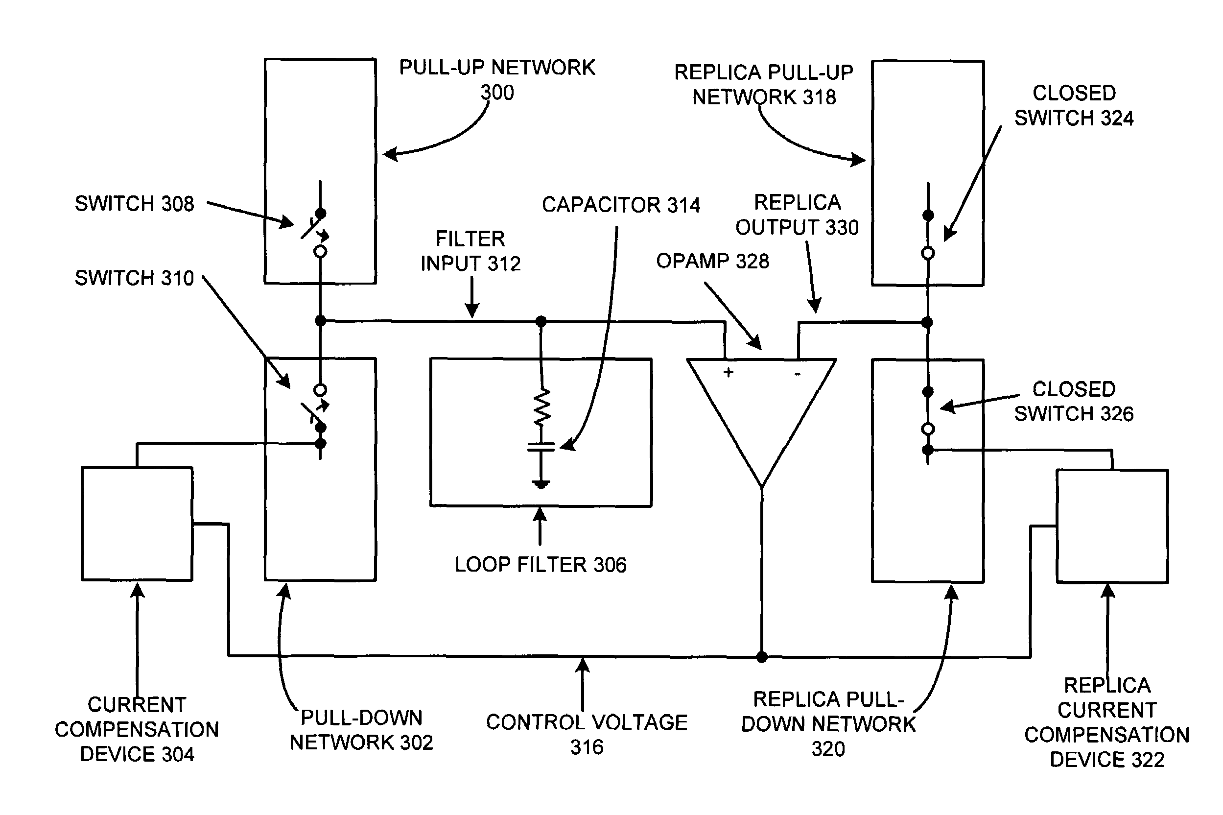
[0031]FIG. 3A presents a block diagram of a charge pump connected to a loop filter in accordance with an embodiment of the present invention. It includes pull-up network 300, pull-down network 302, current compensation device 304, switch 308, switch 310, loop filter 306, filter input 312, capacitor 314, control voltage 316, replica pull-up n...


PUM


Abstract

An apparatus that minimizes phase error and jitter in a phase-locked loop. The apparatus includes a phase/frequency detector, a charge pump, a loop filter, a voltage-controlled oscillator, and a frequency divider, which are coupled together to form a phase-locked loop. The charge pump within the phase-locked loop contains a pull-up network and a pull-down network which are coupled to each other, and a current compensation device. If the pull-up network and the pull-down network are both conducting, the current compensation device adjusts currents flowing through the pull-up network and through the pull-down network such that the currents are substantially equal. This ensures that very little current flows into the loop filter, thereby substantially minimizing a build-up of charge on a capacitor in the loop filter, which can cause phase error and jitter in the phase-locked loop.

Description

BACKGROUND[0001]1. Field of the Invention[0002]The present invention relates to techniques for minimizing phase error and jitter in a phased-locked loop circuit. More specifically, the present invention relates to a phase-locked loop with a charge pump that has a current compensation mechanism that substantially equalizes current flowing through a pull-up network and through a pull-down network to minimize phase error and jitter in the phase-locked loop.[0003]2. Related Art[0004]Advances in semiconductor fabrication technology presently make it possible to integrate large-scale systems, including tens of millions of transistors, into a single semiconductor chip. Integrating such large-scale systems onto a single semiconductor chip enables increases in the frequency at which such systems can operate, because signals between system components do not have to cross chip boundaries, and are not subject to lengthy chip-to-chip propagation delays.[0005]Increasing the operating frequency of...

Claims


Application Information

Patent Timeline
Patent Type & Authority Patents(United States)
IPC IPC(8): H03L7/00G05F3/02H03L7/08
CPCH03L7/0893
Inventor CHEN, YEN-CHUNG T.NAGARAKANTI, KAILASHNATHOH, SUNG-HUN
Owner ORACLE INT CORP
Why Eureka
Try Eureka