Semiconductor chip assembly with solder-attached ground plane
Inactive Publication Date: 2007-07-17
BRIDGE SEMICON
View PDF34 Cites 30 Cited by
Summary
Abstract
Description
Claims
Application Information
AI Technical Summary
This helps you quickly interpret patents by identifying the three key elements:
Problems solved by technology
Method used
Benefits of technology
Benefits of technology
[0081]An advantage of the present invention is that the semiconductor chip assembly can be manufactured conveniently and cost-effectively. Another advantage is that the encapsulant can be provided before the metal base is etched, thereby enhancing mechanical support and protection for the routing line after the pillar is formed. Another advantage is that the pillar can be formed using etching (i.e., subtractively) rather than by electroplating or electroless plating (i.e., additively) which improves uniformity and reduces manufacturing time and cost. Another advantage is that the assembly can include a connection joint made from a wide variety of materials and processes, thereby making advantageous use of mature connection joint technologies in a unique and improved manufacturing approach. Another advantage is that the assembly can be manufactured using low temperature processes which reduces stress and improves reliability. A further advantage is that the assembly can be manufactured using well-controlled processes which can be easily implemented by circuit board, lead frame and tape manufacturers. Still another advantage is that the assembly can be manufactured using materials that are compatible with copper chip and lead-free environmental requirements.
Problems solved by technology
Cross-talk can increase signal line impedance, signal transmission delays and impedance mismatching leading to uncontrolled signal reflections.
Thus, cross-talk is a critical problem that requires some form of compensation.
However, the chip is typically mechanically attached to the flag by solder, which can run-out from underneath the chip.
In addition, the chip is typically electrically connected to the flag by a lengthy wire bond, which can increase inductance and reduce power efficiency.
However, it is difficult to orient and mechanically assemble the chip, the lead frame and the ground plane before the encapsulant is formed to provide a mechanically stable structure.
Method used
Image
Click on the blue label to locate the original text in one second.
Reading with bidirectional positioning of images and text.
Examples
first embodiment
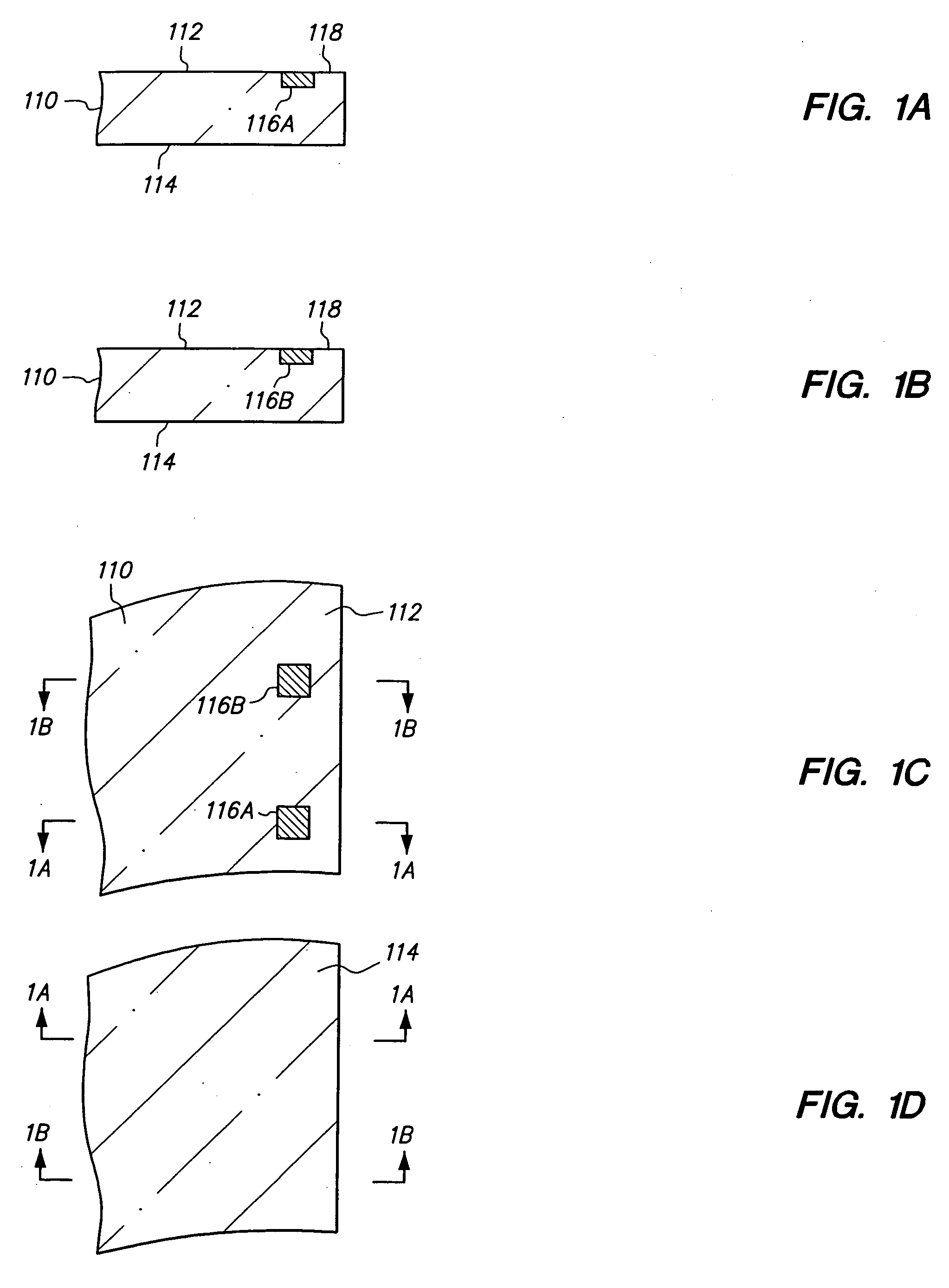
[0102]FIGS. 1A-31A, 1B-31B, 1C-31C and 1D-31D are cross-sectional, cross-sectional, top and bottom views, respectively, of a method of making a semiconductor chip assembly in accordance with the present invention.
[0103]FIGS. 1A, 1B, IC and 1D are cross-sectional, cross-sectional, top and bottom views, respectively, of semiconductor chip 110 which is an integrated circuit in which various transistors, circuits, interconnect lines and the like are formed (not shown). Chip 110 includes opposing major surfaces 112 and 114 and has a thickness (between surfaces 112 and 114) of 150 microns. Surface 112 is the active surface and includes conductive pads 116A and 116B and passivation layer 118. Pads 116A and 116B provide bonding sites to electrically couple chip 110 with external circuitry. Pad 116A is a ground pad, and pad 116B is an input / output pad.
[0104]Pads 116A and 116B are substantially aligned with passivation layer 118 so that surface 112 is essentially flat. Alternatively, pads 116...
seventh embodiment
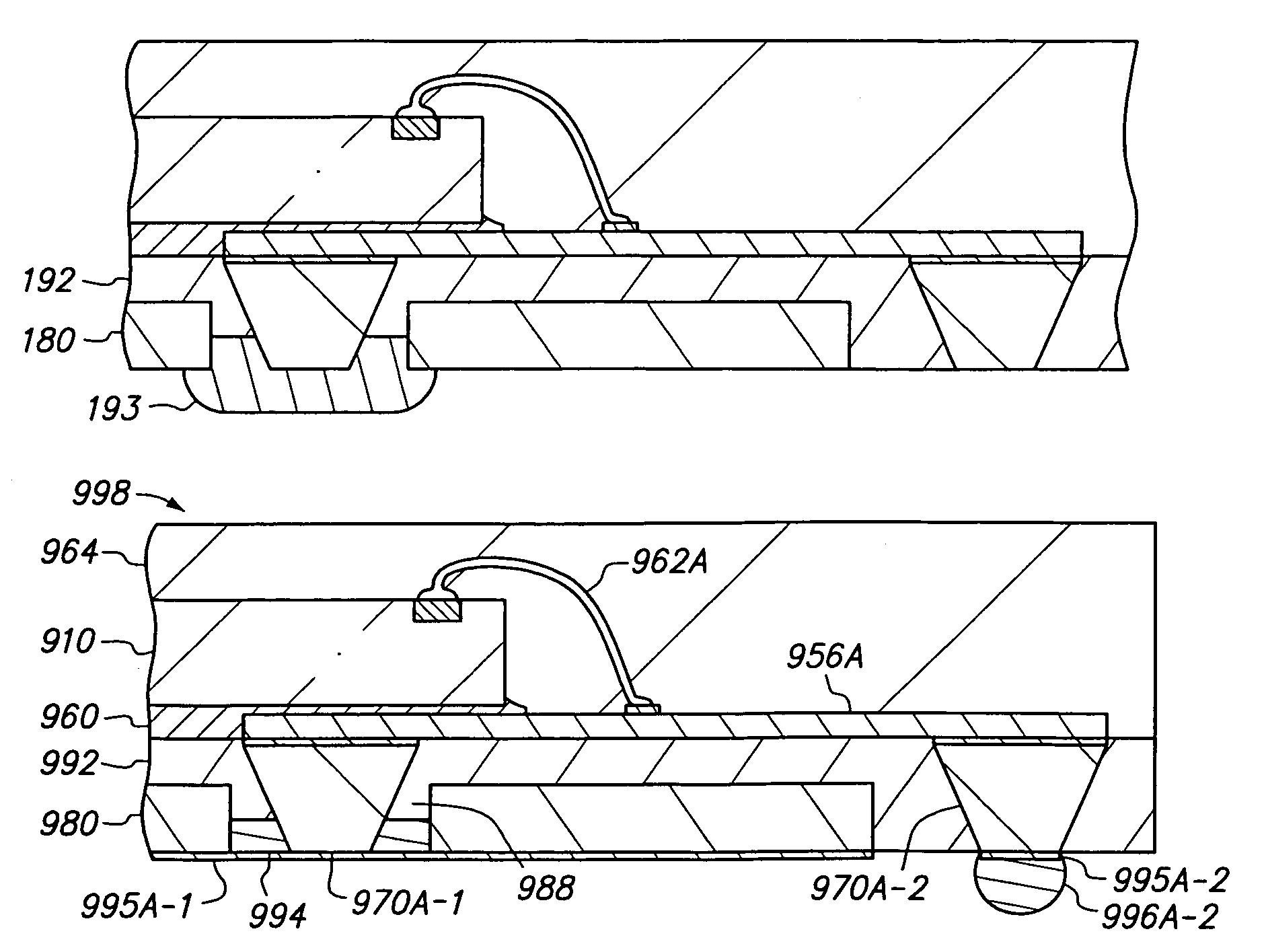
[0280]The pillar (corresponding to pillar 170A-2) is omitted. Furthermore, the elongated region (corresponding to elongated region 146A) is shortened, and the enlarged circular region (corresponding to enlarged circular region 148A-2), the metalcoating (corresponding to metalcoating 194A-2) and the solder ball (corresponding to solder ball 196A-2) are also omitted. This is accomplished in the manner previously described for the
fifth embodiment
[0281]Solder joint 894 is disposed within opening 888. This is accomplished in the manner previously described for the
[0282]Thereafter, solder balls 896A-1 and 896B are formed on solder joint 894 and pillar 870B, respectively.
[0283]Semiconductor chip assembly 898 includes chip 810, routing lines 856A and 856B, adhesive 860, connection joints 862A and 862B, encapsulant 864, pillars 870A-1 and 870B, ground plane 880, insulative base 892, solder joint 894 and solder balls 896A-1 and 896B.
[0284]FIGS. 39A, 39B, 39C and 39D are cross-sectional, cross-sectional, top and bottom views, respectively, of a semiconductor chip assembly in accordance with a ninth embodiment of the present invention. In the ninth embodiment, a metal coating is formed on the pillar that is solder-attached to the ground plane, the solder joint and the ground plane. For purposes of brevity, any description in the first embodiment is incorporated herein insofar as the same is applicable, and the same description need ...
PUM
Abstract
A semiconductorchipassembly includes a semiconductorchip that includes a conductive pad, a conductive trace that includes a pillar and a routing line, a solder joint and a ground plane. The pillar extends into an opening in the ground plane, the solder joint contacts and electrically connects the pillar and the ground plane, and the ground plane is electrically connected to the pad.
Description
CROSS-REFERENCE TO RELATED APPLICATIONS[0001]This application is a continuation-in-part of U.S. application Ser. No. 10 / 866,393 filed Jun. 11, 2004, which is incorporated by reference.BACKGROUND OF THE INVENTION[0002]1. Field of the Invention[0003]The present invention relates to a semiconductorchipassembly, and more particularly to a semiconductor chipassembly with a ground plane and its method of manufacture.[0004]2. Description of the Related Art[0005]Semiconductor chips have power, ground and input / output pads that must be connected to external circuitry in order to function as part of an electronic system. The connection media is typically an array of metallic leads (e.g., a lead frame) or a support circuit (e.g., a substrate), although the connection can be made directly to a circuit panel (e.g., a mother board). Several connection techniques are widely used. These include wire bonding, tape automated bonding (TAB) and flip-chip bonding.[0006]First-level packages include a ...
Claims
Application Information
Patent Timeline
Application Date:The date an application was filed.
Publication Date:The date a patent or application was officially published.
First Publication Date:The earliest publication date of a patent with the same application number.
Issue Date:Publication date of the patent grant document.
PCT Entry Date:The Entry date of PCT National Phase.
Estimated Expiry Date:The statutory expiry date of a patent right according to the Patent Law, and it is the longest term of protection that the patent right can achieve without the termination of the patent right due to other reasons(Term extension factor has been taken into account ).
Invalid Date:Actual expiry date is based on effective date or publication date of legal transaction data of invalid patent.

