
Apparatus and method for signal bus line layout in semiconductor device

a technology of signal bus and layout approach, which is applied in the direction of electrical apparatus, semiconductor devices, semiconductor/solid-state device details, etc., can solve the problems of circuit power noise problems and power noise that is particularly high in certain regions of the device, and achieve the effect of eliminating the power noise drawbacks of the prior approach

Inactive Publication Date: 2007-07-17
SAMSUNG ELECTRONICS CO LTD
View PDF6 Cites 0 Cited by
  • Summary
  • Abstract
  • Description
  • Claims
  • Application Information

AI Technical Summary

Benefits of technology

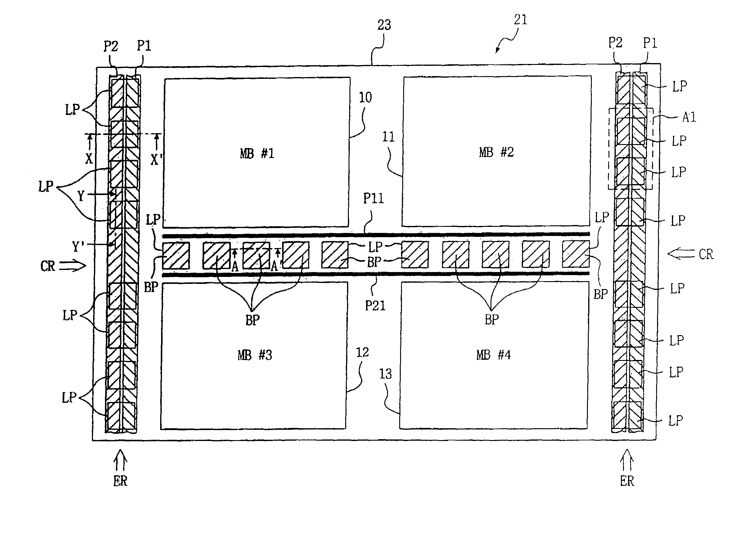
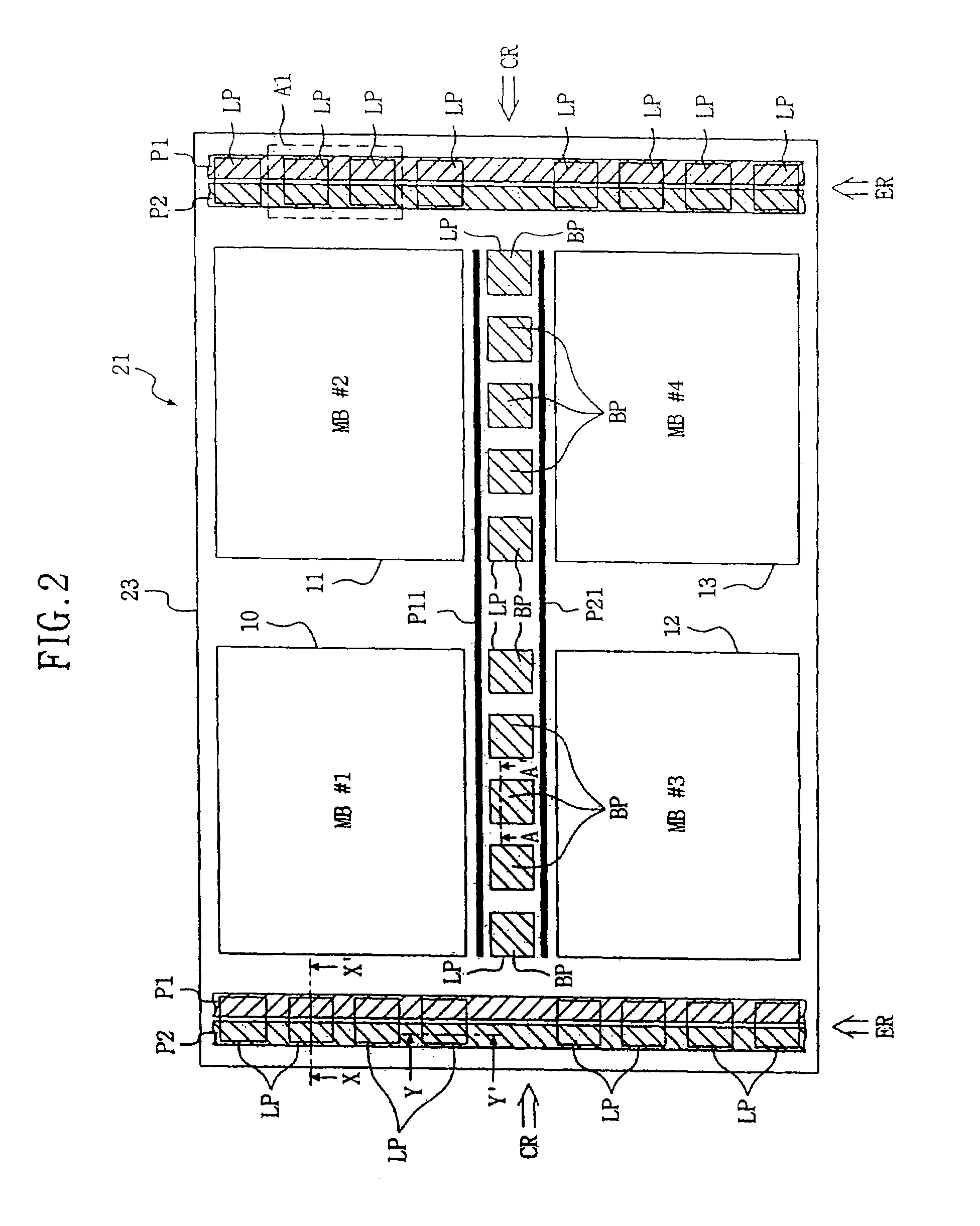
The present invention provides a new approach to laying out and fabricating power bus lines in an integrated circuit device. By forming bonding pads over landing pads and forming power supply lines over the bonding pads, power noise drawbacks are eliminated. The bonding pads and power supply lines can be formed in different directions, allowing for larger portions of the device to be used for power. The device can be used in a board on chip (BOC) configuration or a multichip package (MCP) configuration. The method of manufacturing the semiconductor device includes forming a plurality of landing pads, forming a plurality of bonding pads over a first portion of the landing pads, and forming a power supply line over a second portion of the landing pads.

Problems solved by technology

For example, because of the relatively low conductivity of the small power bus lines, the circuit can experience power noise problems.
The power noise can be particularly high in certain particular regions of the device, depending on whether the device is connected in an edge pad configuration or a center pad configuration.

Method used


Image

  • Apparatus and method for signal bus line layout in semiconductor device
  • Apparatus and method for signal bus line layout in semiconductor device
  • Apparatus and method for signal bus line layout in semiconductor device

Examples


Embodiment Construction

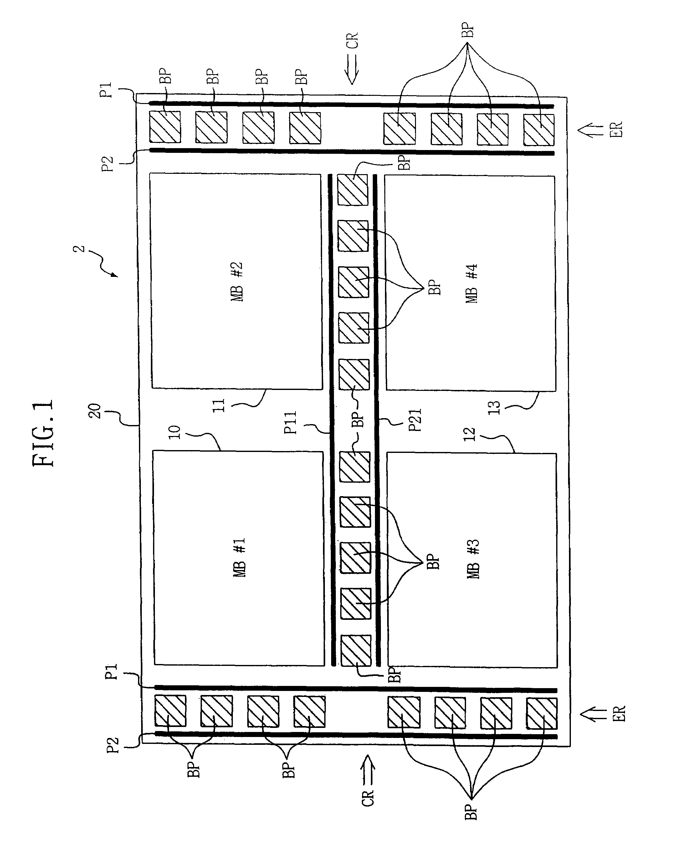
[0048]FIG. 1 is a schematic diagram illustrating a layout of bonding pads and power supply bus lines in a conventional semiconductor memory device. The device 2 includes a plurality of memory blocks 10, 11, 12 and 13 on a substrate 20. A center region CR is defined between the memory blocks as shown, and edge regions ER are defined between the memory blocks and the edges of the substrate 20. A plurality of bonding pads BP are formed in both the edge regions ER and the center region CR as shown. In each of the regions, a pair of power supply bus lines is also formed. Specifically, in the edge regions ER, power supply bus lines P1 and P2 are formed on opposite sides of the bonding pads BP, and power supply bus lines P11 and P21 are formed in the center region on opposite sides of the bonding pads BP.

[0049]The device in FIG. 1 is fabricated to accommodate both a center pad configuration and an edge pad configuration. Accordingly, bonding pads BP as well as power supply lines P1, P2, P1...


PUM


Abstract

A device and method for layout and fabrication of power supply bus lines in an integrated circuit such as a memory circuit are described. In accordance with the present invention, power bus lines and bonding pads of the circuit are not necessarily formed in both edge regions and center regions of the device. The bonding pads are formed in the region according to the package being used, and the power bus lines are formed in the other region. This is accomplished by forming the bonding pads over landing pads. Landing pads are formed in both the center region and the edge region under the top surface of the device. If the device is to be packaged in an edge pad configuration, the bonding pads are formed over the landing pads in the edge region, and power supply bus lines can be formed over the landing pads in the center region. Similarly, if the device is to be packaged in a center pad configuration, the bonding pads are formed over the landing pads in the center region, and the power supply bus lines can be formed over the landing pads in the edge region. The bonding pads are connected to the landing pads by conductive vias. Because the power bus lines are not formed in the same region as bonding pads, they can occupy a relatively large portion of the region in which they are formed. That is, they can be made much larger than they would be using the conventional approach in which both bonding pads and power bus lines are formed in the same region. As a result, the power noise drawbacks of the conventional approach are eliminated.

Description

RELATED APPLICATION[0001]This application relies for priority on Korean Patent Application number 2003-39163, filed on Jun. 17, 2003, the contents of which are incorporated herein in their entirety by reference.FIELD OF THE INVENTION[0002]The invention relates to a signal bus line layout approach in a semiconductor device, and, more particularly, to an approach for efficiently laying out a power bus line in a semiconductor device such as a memory device to reduce power noise while not increasing chip size.BACKGROUND OF THE INVENTION[0003]Many semiconductor devices include multiple circuits such as memory blocks disposed in a two-dimensional array. The array of circuits defines an edge region at the edges of the array of circuits and a center region between the circuits. Typically, connections are made in either or both of the edge region and the center region. To that end, bonding pads are typically formed in both regions. Also, power bus lines must be routed throughout the device, ...

Claims


Application Information

Patent Timeline
Patent Type & Authority Patents(United States)
IPC IPC(8): H01L23/48H01L21/60H01L23/485H01L23/528
CPCH01L23/5286H01L24/06H01L2924/01039H01L2924/01046H01L2924/01074H01L2924/01024H01L2924/01033H01L2924/01068H01L2924/14H01L2224/02166H01L2224/05554H01L21/60
Inventor LEE, CHANG-HOCHOI, JONG-HYUN
Owner SAMSUNG ELECTRONICS CO LTD
Learn More