Process for fabricating an integrated circuit package
What is Al technical title?
Al technical title is built by PatSnap Al team. It summarizes the technical point description of the patent document.
a technology of integrated circuits and manufacturing processes, applied in the direction of electrical equipment, semiconductor devices, semiconductor/solid-state device details, etc., can solve the problems of reducing manufacturing costs, achieve better board mount reliability, reduce manufacturing costs, and increase rigidity and suppor
Inactive Publication Date: 2007-07-24
UTAC HEADQUARTERS PTE LTD
View PDF41 Cites 135 Cited by
Summary
Abstract
Description
Claims
Application Information
AI Technical Summary
This helps you quickly interpret patents by identifying the three key elements:
Problems solved by technology
Method used
Benefits of technology
[0009]Advantageously, the unique etch-back process results in mold interlocking features for better board mount reliability. Also, the mold interlocking features are provided by an etch-back process that results in decreased cost of manufacture as compared to plate-up processes.
[0010]In one aspect, the package is manufactured using a carrier strip that is laminated to the leadframe strip. Advantageousl
Problems solved by technology
Also, the mold interlocking features are provided by an etch-back process tha
Method used
Image
Click on the blue label to locate the original text in one second.
Reading with bidirectional positioning of images and text.
Examples
Embodiment Construction
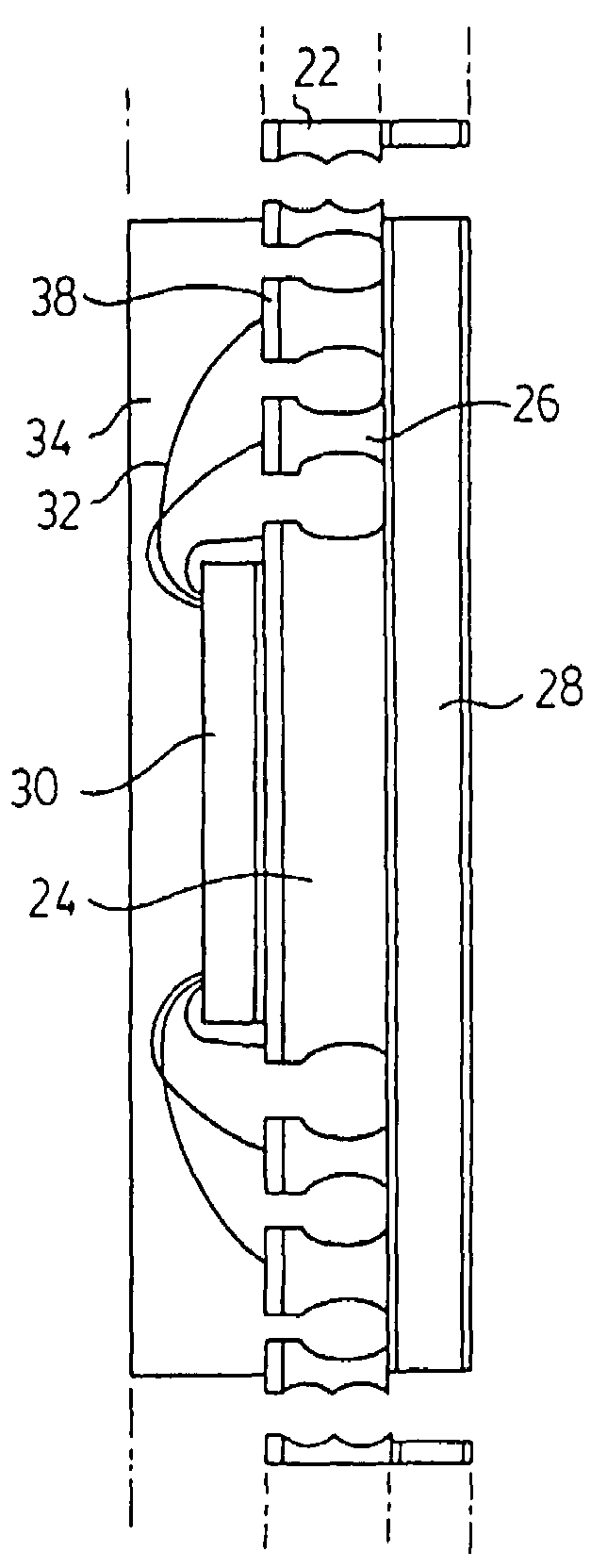
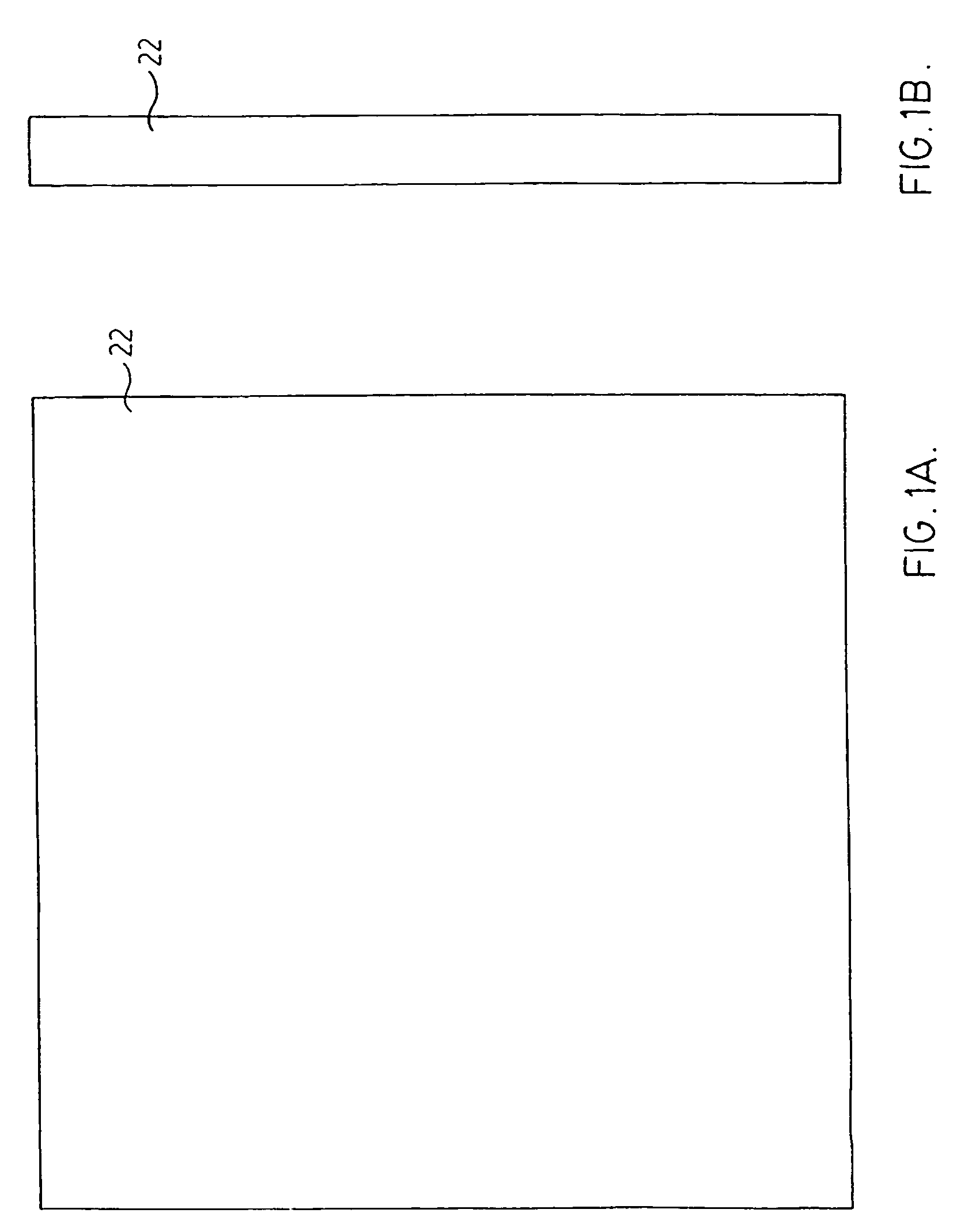
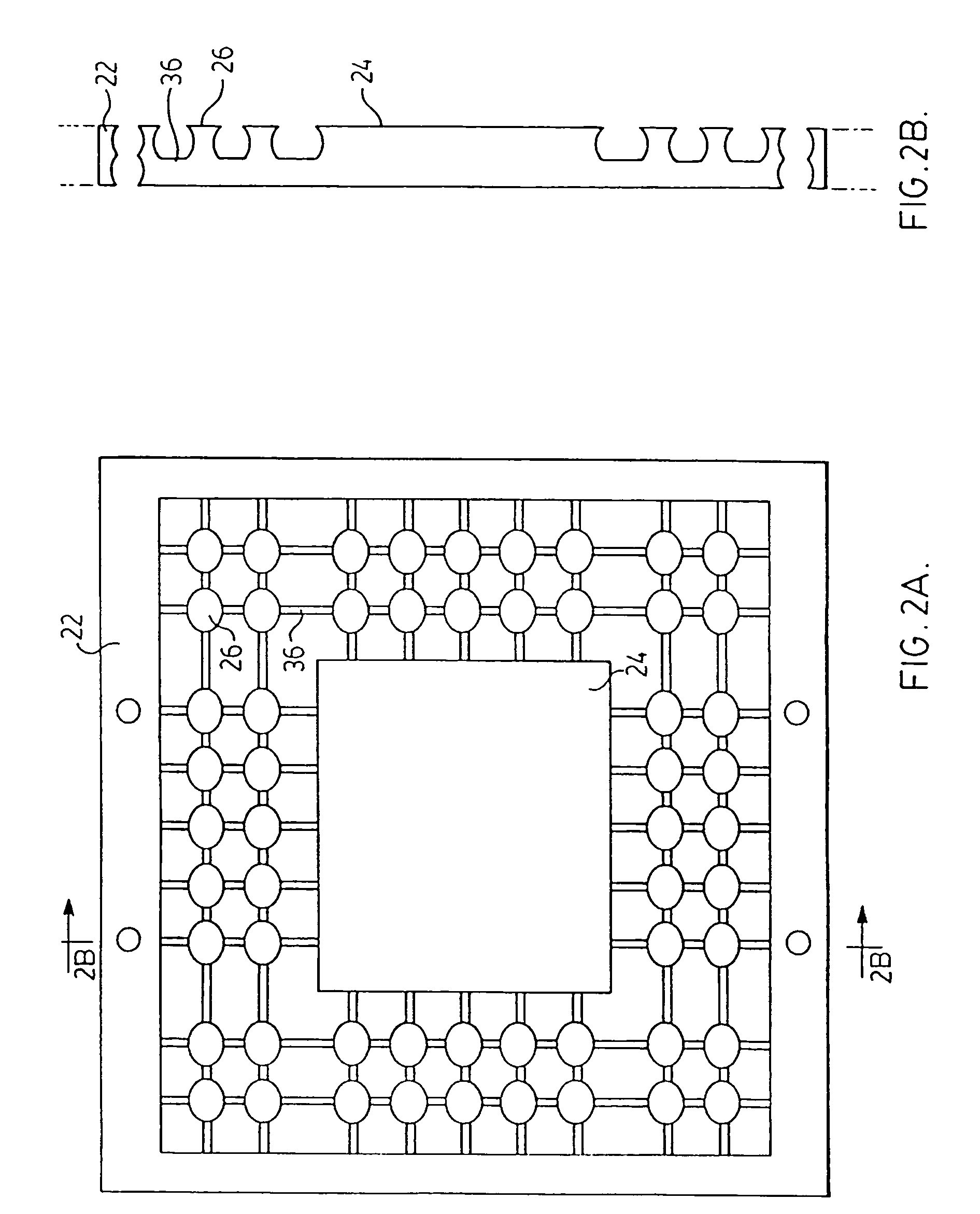
[0014]Reference is first made to FIGS. 1 to 11 to describe a process for fabricating an integrated circuit package, indicated generally in FIG. 11 by the numeral 20. The process includes selectively etching at least a first side of a leadframe strip 22 to define portions of a die attach pad 24 and at least one row of contacts 26 adjacent the die attach pad 24. A carrier strip 28 is laminated to the first side of the leadframe strip 22 and a second side of the leadframe strip 22 is selectively etched to thereby define a remainder of the die attach pad 24 and the at least one row of contacts 26. A semiconductor die 30 is mounted to the die attach pad 24, on the second side of the leadframe strip 22 and the semiconductor die 30 is wire bonded to ones of the contacts 26. The second side of the leadframe strip 22 is encapsulated, including the semiconductor die 30 and wire bonds 32, in a molding material 34. The carrier strip 28 is removed from the leadframe strip 22 and the integrated c...
PUM
Abstract
A process for fabricating an integrated circuit package. At least a first side of a leadframe strip is selectively etched to define portions of a die attach pad and at least one row of contacts adjacent the die attach pad. A carrier strip is laminated to the first side of the leadframe strip and a second side of the leadframe strip is selectively etched to thereby define a remainder of the die attach pad and the at least one row of contacts. A semiconductor die is mounted to the die attach pad, on the second side of the leadframe strip and the semiconductor die is wire bonded to ones of the contacts. The second side of the leadframe strip is encapsulating, including the semiconductor die and wire bonds, in a molding material. The carrier strip is removed from the leadframe strip and the integrated circuit package is singulated from a remainder of the leadframe strip.
Description
CROSS-REFERENCE TO RELATED APPLICATIONS[0001]This is a continuation-in-part of U.S. patent application Ser. No. 10 / 765,192, filed Jan. 28, 2004, now U.S. Pat. No. 7,049,177 entitled Leadless Plastic Chip Carrier with Standoff Contacts and Die Attach Pad and a continuation-in-part of U.S. patent application Ser. No. 09 / 802,678, filed Mar. 9, 2001, now U.S. Pat. No. 6,933,594 which is a continuation-in-part of U.S. patent application Ser. No. 09 / 288,352, filed Apr. 8, 1999 now U.S. Pat. No. 6,498,099, issued Dec. 24, 2002, which is a continuation-in-part of U.S. patent application Ser. No. 09 / 095,803 filed Jun. 10, 1998, now U.S. Pat. No. 6,299,200, issued May 8, 2001.FIELD OF THE INVENTION[0002]The present invention relates in general to integrated circuit packaging and more particularly to an improved process for fabricating an integrated circuit package, that includes unique features that allow gang testing of integrated circuit packages and etching to provide mold interlock.BACKGR...
Claims
Application Information
Patent Timeline
Application Date:The date an application was filed.
Publication Date:The date a patent or application was officially published.
First Publication Date:The earliest publication date of a patent with the same application number.
Issue Date:Publication date of the patent grant document.
PCT Entry Date:The Entry date of PCT National Phase.
Estimated Expiry Date:The statutory expiry date of a patent right according to the Patent Law, and it is the longest term of protection that the patent right can achieve without the termination of the patent right due to other reasons(Term extension factor has been taken into account ).
Invalid Date:Actual expiry date is based on effective date or publication date of legal transaction data of invalid patent.