Alloy type semiconductor nanocrystals and method for preparing the same

a technology of alloy-type semiconductors and nanocrystals, which is applied in the field of alloy-type semiconductor nanocrystals, can solve the problems of difficult fabrication of commercially available semiconductor devices, limited solvent methods, and difficult formation of reproducible and uniform quantum structures in solvents containing a large amount of impurities, and achieves high quantum efficiency and uniform sizes and shapes

Active Publication Date: 2007-07-31
SAMSUNG ELECTRONICS CO LTD
View PDF10 Cites 32 Cited by
  • Summary
  • Abstract
  • Description
  • Claims
  • Application Information

AI Technical Summary

Benefits of technology

[0011]The present invention provides alloy type Group 12-16 compound semiconductor nanocrystals which are stable and have a high quantum efficiency and uniform sizes and shapes.
[0012]The present invention also provides a simple, reproducible, chemical wet preparation method for the alloy type Group 12-16 compound semiconductor nanocrystals.
[0013]The present invention also provides an organic electroluminescent (EL) device with good luminance characteristics using the Group 12-16 compound semiconductor nanocrystals.

Problems solved by technology

Even though quantum dots grown mainly by lattice mismatch using a vapor phase method have good crystallinity, the vapor phase method has a fatal defect in controlling the size, uniformity, and density of the quantum dots, which renders fabrication of commercially available semiconductor devices difficult.
However, this method has a restriction on the solvent used, i.e., tri-octyl phophonic acid (referred to as TOPO, hereinafter).
Reportedly, it is difficult to form reproducible and uniform quantum structures in a solvent containing a large amount of impurities.
It is also reported that impurities in the technical grade TOPO serves as an uncontrollable reaction parameter that adversely affects the reaction.
In this case, however, a change in a binding property of TOPO may occur, which renders the growth of desired crystals difficult.

Method used


Image

  • Alloy type semiconductor nanocrystals and method for preparing the same
  • Alloy type semiconductor nanocrystals and method for preparing the same
  • Alloy type semiconductor nanocrystals and method for preparing the same

Examples


example 1

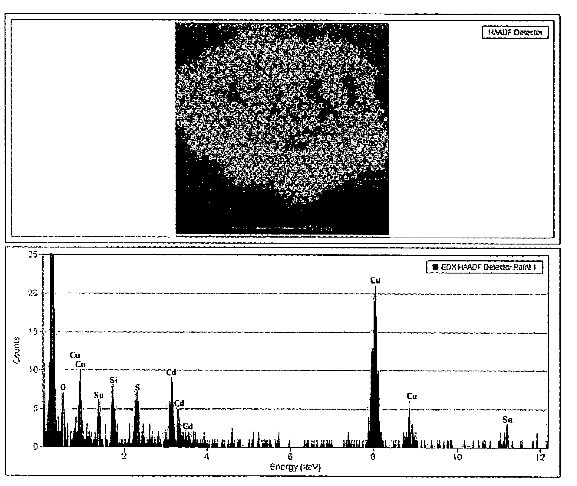
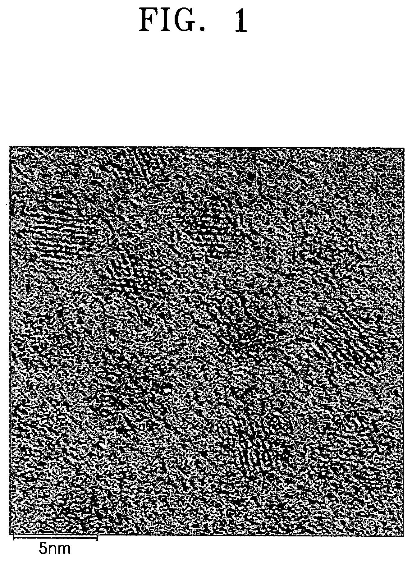
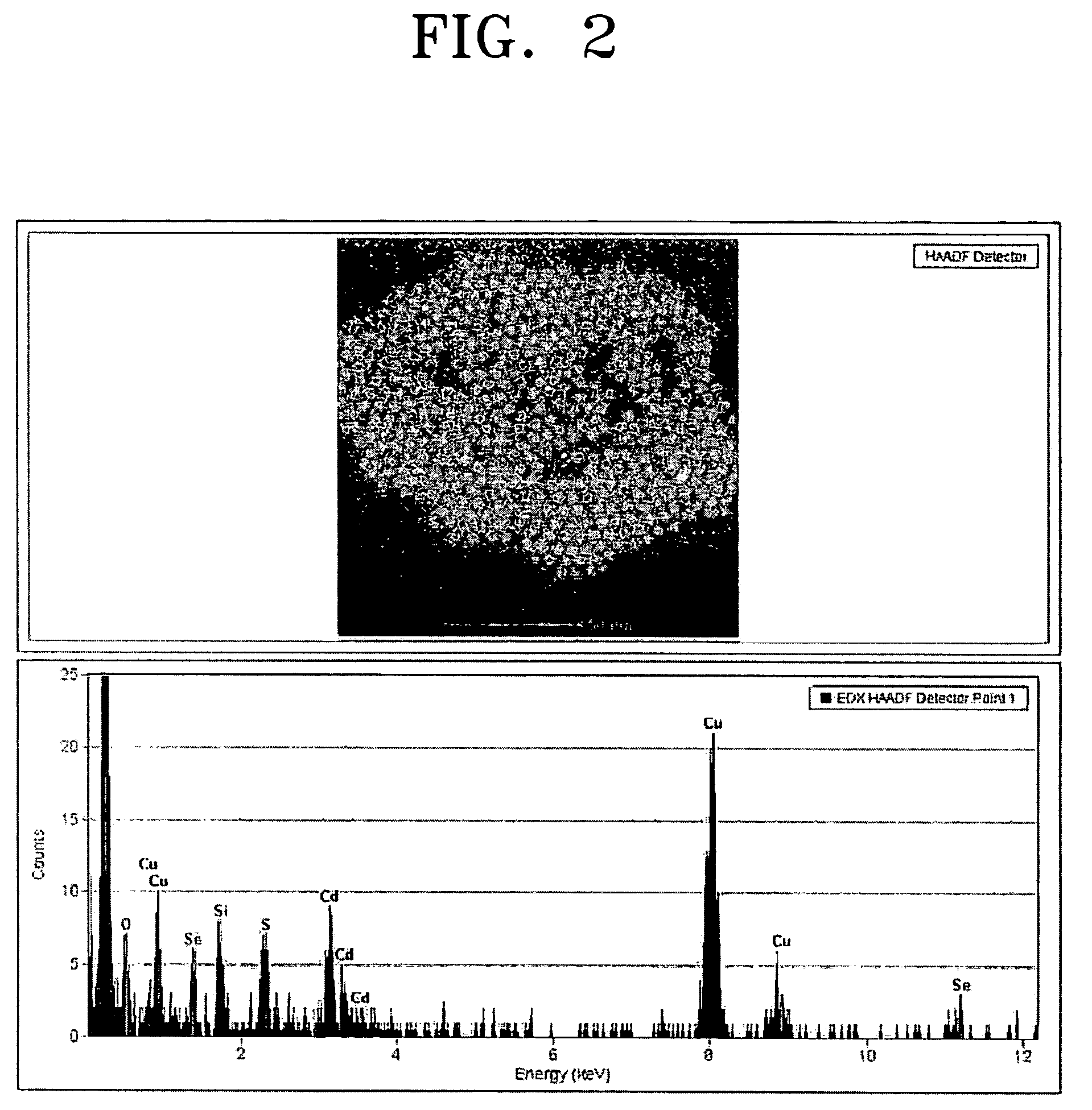
Preparation of CdSeS Nanocrystals

[0063]16 g of tri-octyl amine (referred to as TOA, hereinafter), 0.5 g of oleic acid, and 0.4 mmol of CdO were simultaneously placed in a 100 ml flask provided with a reflux condenser and stirred at 300° C. to obtain a Cd precursor solution.

[0064]Separately, Se powders were dissolved in tri-octyl phosphine (referred to as TOP, hereinafter) to obtain a Se-TOP complex solution with a Se concentration of about 0.1M. S powders were dissolved on TOP to obtain S-TOP complex solution with a S concentration of about 4M.

[0065]0.5 ml of S-TOP complex solution 0.5 ml of the Se-TOP complex solution were rapidly added to the Cd precursor solution and stirred for about 4 minutes.

[0066]When the reaction of the resultant mixture was terminated, the reaction temperature was rapidly reduced to room temperature and then centrifugation was performed with addition of an ethanol as a non-solvent. A supernatant was decanted and discarded. A precipitate was dispersed in a t...

example 2

Preparation of ZnCdSe Nanocrystals

[0072]16 g of TOA, 0.5 g of oleic acid, 0.2 mmol of zinc acetyl acetonate, and 0.2 mmol of cadmium (Cd) oxide were simultaneously placed in a 100 ml flask provided with a reflux condenser and stirred at 300° C. to obtain a Zn and Cd precursor solution.

[0073]Separately, Se powders were dissolved in TOP to obtain a Se-TOP complex solution with a Se concentration of about 0.25M. 1 ml of the Se-TOP complex solution was rapidly added to the Zn and Cd precursor solution and stirred for about 2 minutes.

[0074]When the reaction of the resultant mixture was terminated, the reaction temperature was rapidly reduced to room temperature and then centrifugation was performed with addition of an ethanol as a non-solvent. A supernatant was decanted and discarded. A precipitate was dispersed in a toluene and then a PL spectrum in the solution was measured.

[0075]The PL spectrum showed an emission wavelength of about 456 nm and FWHM of about 26 nm.

example 3

Preparation of CdSe / CdS Nanocrystals

[0076]16 g of TOA, 0.5 g of oleic acid, and 0.4 mmol of cadmium acetate were simultaneously placed in a 100 ml flask provided with a reflux condenser and stirred at 300° C. to obtain a Cd precursor solution.

[0077]Separately, Se powders were dissolved in TOP to obtain a Se-TOP complex solution with a Se concentration of about 0.25M. 1 ml of the Se-TOP complex solution was rapidly added to the Cd precursor solution and stirred for about 4 minutes.

[0078]S powders were dissolved in TOP to obtain a S-TOP complex solution with a S concentration of about 2 M. 1 ml of the S-TOP complex solution was dropwise added to the CdSe-containing solution and stirred.

[0079]When the reaction of the resultant mixture was terminated, the reaction temperature was rapidly reduced to room temperature and then centrifugation was performed with addition of an ethanol as a non solvent. A supernatant was decanted and discarded. A precipitate was dispersed in a toluene and the...


PUM

PropertyMeasurementUnit
molar ratioaaaaaaaaaa
temperatureaaaaaaaaaa

Abstract

Provided is a chemical wet preparation method for Group 12-16 compound semiconductor nanocrystals. The method includes mixing one or more Group 12 metals or Group 12 precursors with a dispersing agent and a solvent followed by heating to obtain a Group 12 metal precursor solution; dissolving one or more Group 16 elements or Group 16 precursors in a coordinating solvent to obtain a Group 16 element precursor solution; and mixing the Group 12 metal precursors solution and the Group 16 element precursors solution to form a mixture, and then reacting the mixture to grow the semiconductor nanocrystals. The Group 12-16 compound semiconductor nanocrystals are stable and have high quantum efficiency and uniform sizes and shapes.

Description

BACKGROUND OF THE INVENTION[0001]This application claims priority from Korean Patent Application No. 2003-49547, filed on Jul. 19, 2003, in the Korean Intellectual Property Office, the disclosure of which is incorporated herein in its entirety by reference.[0002]1. Field of the Invention[0003]The present invention relates to alloy type semiconductor nanocrystals and a method of preparing the same. More particularly, the present invention relates to alloy type Group 12-16 compound semiconductor nanocrystals with a high luminance efficiency in a visible light band and a wet preparation method for the semiconductor nanocrystals.[0004]2. Description of the Related Art[0005]When compound semiconductor materials are made into nanometer-sized crystals, a quantum confinement effect occurs at the regions of the crystals smaller than the bulk exciton Bohr radius. Such a quantum confinement effect results in a change in bandgap energy which is intrinsic characteristics of semiconductor materia...

Claims


Application Information

Patent Timeline
Patent Type & Authority Patents(United States)
IPC IPC(8): B32B5/16C30B7/00H01L21/20B82Y20/00H05B33/14C01B17/20C01B19/00C09K11/00C09K11/08C09K11/56C09K11/88C09K11/89H01L21/208H01L21/368H01L29/06H01L31/0256H01L51/00H01L51/42H01L51/50H05B33/00
CPCB82Y10/00B82Y30/00C01B17/20C01B19/007C09K11/883H01L29/0665H01L29/0673H01L51/5012H05B33/14C30B7/00C30B7/005H01L21/02551H01L21/02557H01L21/0256H01L21/02601H01L21/02628B82Y20/00Y10T428/2982C01P2002/72C01P2002/84C01P2002/85C01P2004/04C01P2004/52H01L51/0059H01L51/0081H01L51/4213Y10S977/777Y10S977/824Y10S977/825Y10S977/784Y10S977/785Y10T428/2991Y10T428/12028Y10T428/12049Y10T428/12181H10K85/631H10K85/324H10K50/11H10K30/10
Inventor JANG, EUN-JOOAHN, TAE-KYUNG
Owner SAMSUNG ELECTRONICS CO LTD
Why Eureka
Try Eureka