MEMS switch and method of fabricating the same

a technology of micro-electromechanical system and switch, which is applied in the direction of electrostatic/electro-adhesion relays, instruments, contacts, etc., can solve the problems of unintentional adhesion, signal transmission is not smooth, and the restoration force fails to overcome the force working on the surface, so as to reduce the stiction failure and the insertion loss, the effect of low voltag

Active Publication Date: 2007-07-31
SAMSUNG ELECTRONICS CO LTD
View PDF3 Cites 6 Cited by
  • Summary
  • Abstract
  • Description
  • Claims
  • Application Information

AI Technical Summary

Benefits of technology

[0012]Accordingly, the present general inventive concept has been made to solve the above-mentioned problems, and an aspect of the present general inventive concept is to provide a MEMS switch which can reduce a stiction fail and an insertion loss and be driven at a low voltage.
[0024]Widths of the second spring arms may be greater than a width of the first spring arm so as to increase the stiffness of the second spring arms.
[0033]The second spring arms may be stiffer than the first spring arm. Widths of the second spring arms may be greater than a width of the first spring arms so as to increase the stiffness of the second spring arms.

Problems solved by technology

In the stiction phenomenon, an unintentional adhesion occurs on a surface of a micro structure, and thus a restoration force fails to overcome a force working on a surface such as a capillary force, a Van der Walls force, an electrostatic force, or the like.
Also, in a case where contact states of the shorting bar disclosed in U.S. Pat. No. 6,307,169 and the short piece disclosed in Japanese Patent Publication No. hei 2001-143595 are poor, signals are not smoothly transmitted, and an insertion loss occurs.

Method used


Image

  • MEMS switch and method of fabricating the same
  • MEMS switch and method of fabricating the same
  • MEMS switch and method of fabricating the same

Examples


Embodiment Construction

[0042]Exemplary embodiments of the present invention will be described in greater detail with reference to the accompanying drawings.

[0043]In the following description, same drawing reference numerals are used for the same elements even in different drawings. The matters defined in the description such as a detailed construction and elements are nothing but the ones provided to assist in a comprehensive understanding of the invention. Thus, it is apparent that the present invention can be carried out without those defined matters. Also, well-known functions or constructions are not described in detail since they would obscure the invention in unnecessary detail.

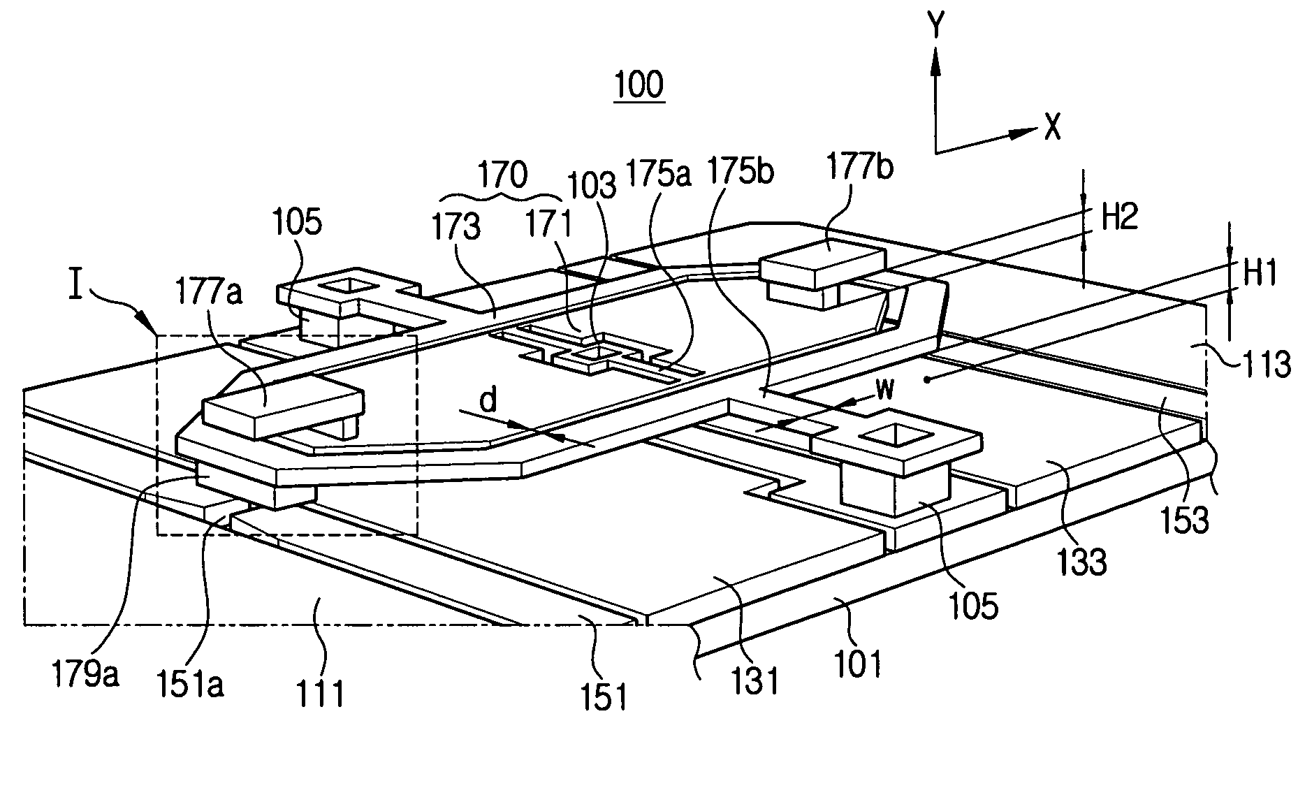
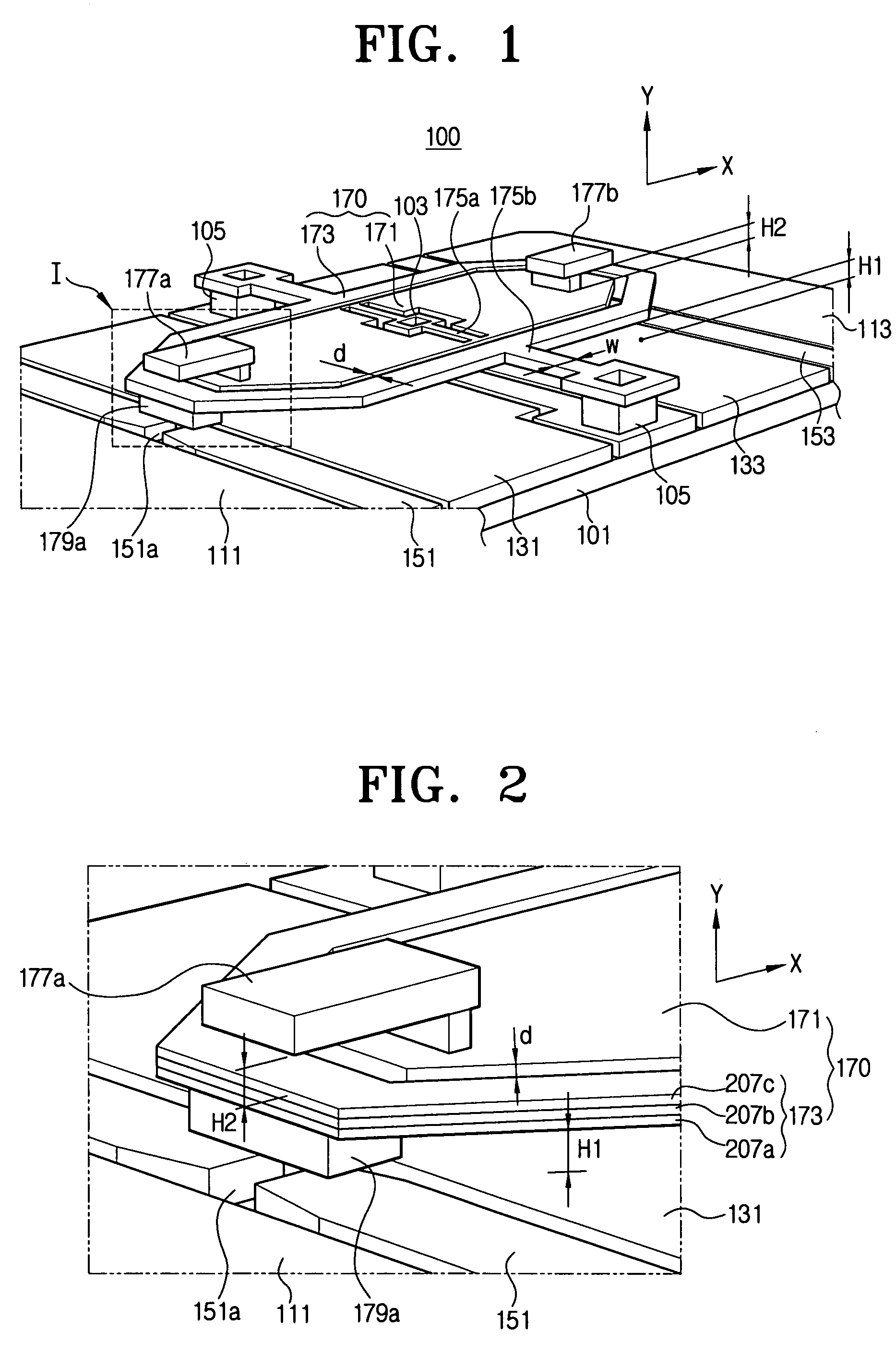
[0044]A MEMS switch shown in the drawings is magnified. In particular, direction Y is exaggerated for description convenience.

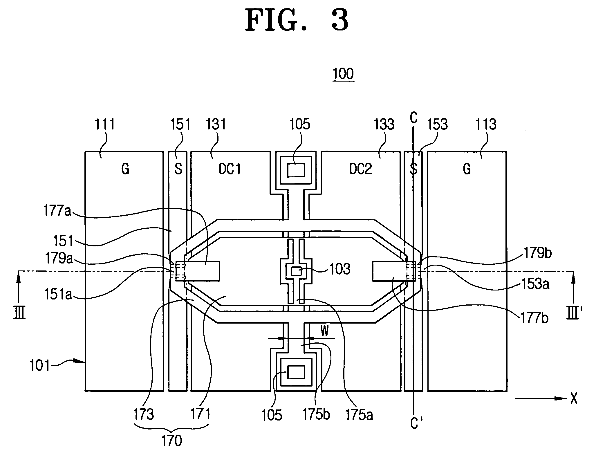
[0045]FIG. 1 is a schematic perspective view of an MEMS switch according to an exemplary embodiment of the present invention, FIG. 2 is an enlarged view of portion I shown in FIG. 1, and FIG. 3 is a pl...


PUM


Abstract

A micro electro mechanical system switch and a method of fabricating the same. The micro electro mechanical system switch includes a substrate a plurality of signal lines formed at sides an upper surface of the substrate and including switching contact points and a plurality of immovable electrodes on the upper surface of the substrate and between the plurality of signal lines. An inner actuating member performs a seesaw based on a center of the substrate and together with an outer actuating member. Pushing rods are formed at ends of an upper surface of the inner actuating member with ends protruding from and overlapping with an upper portion of the outer actuating member. Contacting members are formed on a lower surface of the outer actuating member so as to be pushed by the pushing rods and contacting the switching contact points of the signal lines.

Description

CROSS-REFERENCE TO RELATED APPLICATIONS[0001]This application claims the benefit of Korean Patent Application No. 2004-107858, filed on Dec. 17, 2004, in the Korean Intellectual Property Office, the disclosure of which is incorporated herein by reference.BACKGROUND OF THE INVENTION[0002]1. Field of the Invention[0003]The present invention relates to a Micro Electro Mechanical System (MEMS) switch and a method of fabricating the same.[0004]2. Description of the Related Art[0005]RF switches of radio frequency (RF) devices using MEMS technology are widely manufactured. The RF switches are devices mainly applied to circuits selecting and transmitting signals and matching impedances in wireless telecommunication terminals and systems in a micro wave band or a millimeter wave band.[0006]U.S. Pat. No. 6,307,169 (inventor: Sun et al.) discloses such a MEMS switch.[0007]The disclosed MEMS switch includes a hinge supporting a membrane type electrode on a substrate. The hinge includes a contro...

Claims


Application Information

Patent Timeline
Patent Type & Authority Patents(United States)
IPC IPC(8): G02B26/00H01P1/10
CPCH01H1/5822H01H59/0009H01H2059/0054H01H2059/0063
Inventor KIM, CHE-HEUNGSHIN, HYUNG-JAEKWEON, SOON-CHEOLKIM, KYU-SIKLEE, SANG-HUN
Owner SAMSUNG ELECTRONICS CO LTD
Why Eureka
Try Eureka