Bandgap reference designs with stacked diodes, integrated current source and integrated sub-bandgap reference

a reference circuit and diode technology, applied in the field of electronic circuitry, can solve the problems of small offset error, relatively large error at the amplifier output, and ineffective in some applications, and achieve the effects of improving the performance of the bandgap reference circuit, reducing the input sensitivity of the error amplifier, and increasing the vb

Active Publication Date: 2007-08-07
NAT SEMICON CORP
View PDF5 Cites 25 Cited by
  • Summary
  • Abstract
  • Description
  • Claims
  • Application Information

AI Technical Summary

Benefits of technology

[0006]Exemplary embodiments of the invention improve bandgap reference circuit performance by increasing ΔVBE, and thereby correspondingly decreasing the input sensitivity of the error amplifier in the control loop. Some embodiments increase ΔVBE by presenting stacked diode configurations at the amplifier inputs, other embodiments increase ΔVBE by increasing the diode ratio presented at the amplifier in...

Problems solved by technology

This multiplication factor can translate a relatively small offset error at the amplifier input into a relatively large error at the amplifier output.
Trimming can provide a limited solution to the offset problem, but usually only at a single nominal temperatu...

Method used


Image

  • Bandgap reference designs with stacked diodes, integrated current source and integrated sub-bandgap reference
  • Bandgap reference designs with stacked diodes, integrated current source and integrated sub-bandgap reference
  • Bandgap reference designs with stacked diodes, integrated current source and integrated sub-bandgap reference

Examples


Embodiment Construction

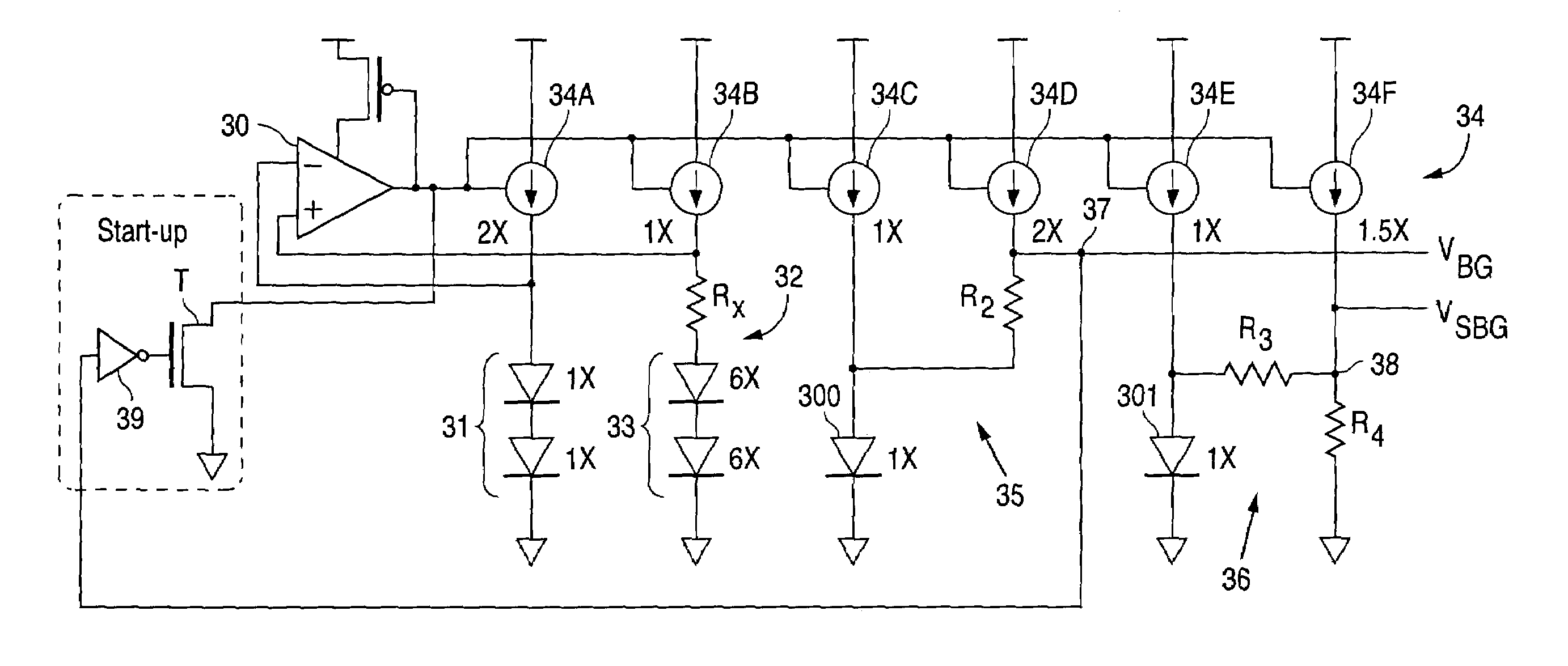
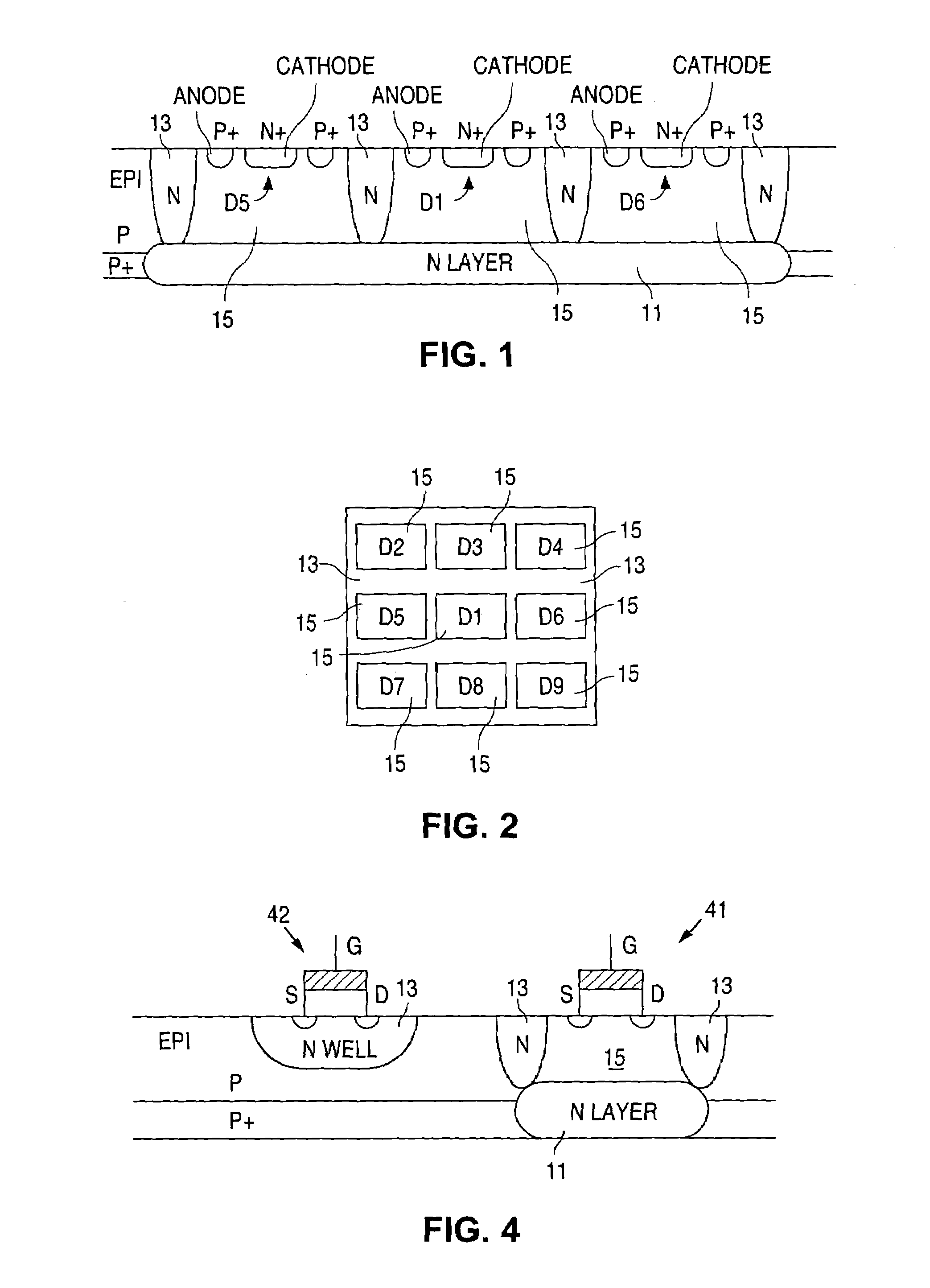
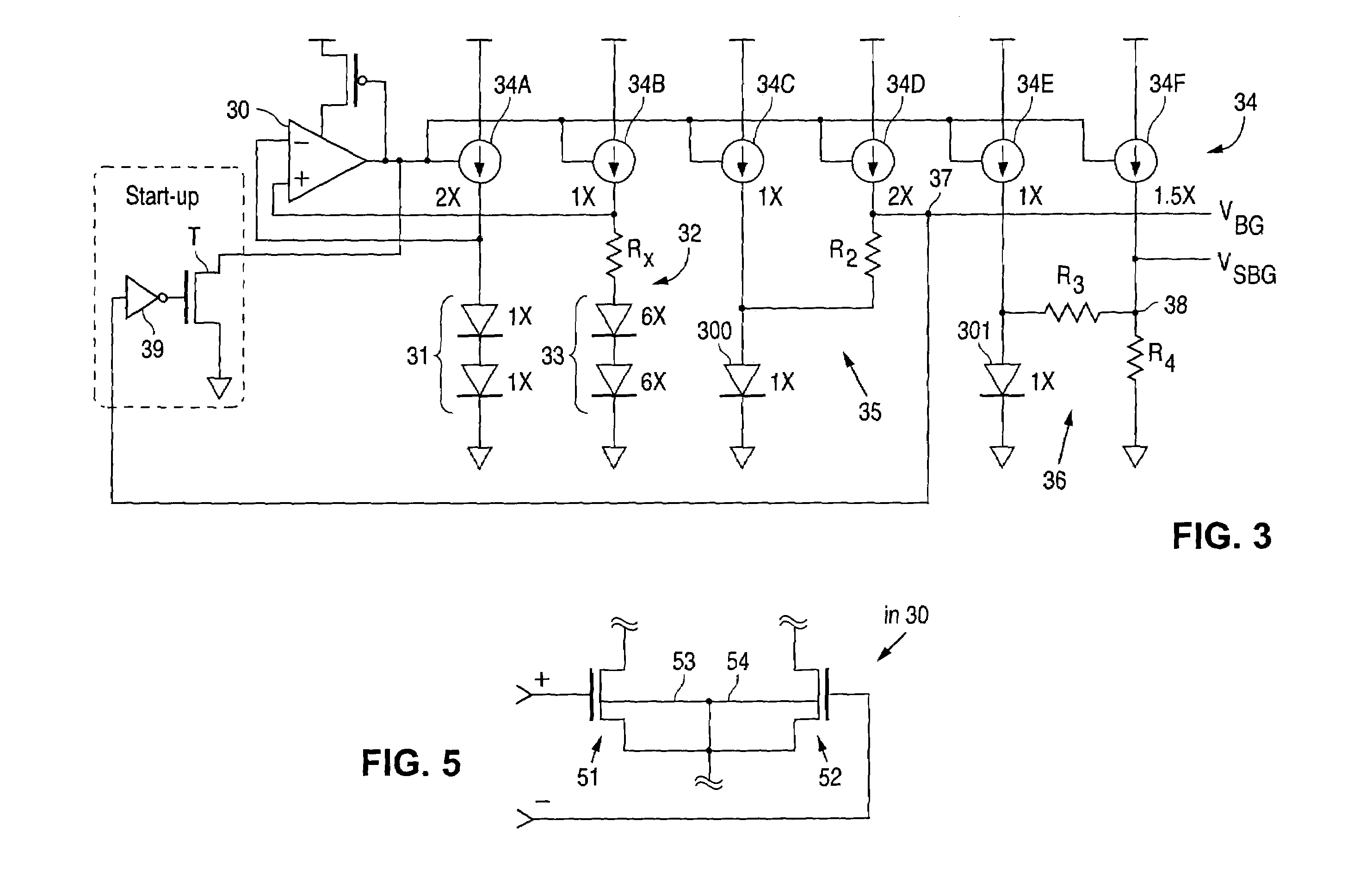
[0015]FIGS. 1 through 6, discussed herein, and the various embodiments used to describe the principles of the present invention in this patent document are by way of illustration only and should not be construed in any way to limit the scope of the invention. Those skilled in the art will understand that the principles of the present invention may be implemented in any suitably arranged system.

[0016]The drop across the resistor in the PTAT (proportional to absolute temperature) leg of a conventional bandgap reference circuit is commonly referenced to as ΔVBE, because it represents the difference between the voltage drops (base-emitter voltages) of the respective diode structures in the PTAT and CTAT (complementary to absolute temperature) legs of the circuit. In a typical conventional bandgap circuit, ΔVBE is around 50 millivolts. The sum of the multiplied ΔVBE and the diode potential (about 0.6 volts) must be equal to approximately 1.22 volts, the bandgap voltage. Accordingly, the ...


PUM


Abstract

The performance of a bandgap reference circuit is improved by increasing the ΔVBE, and thereby correspondingly decreasing the input sensitivity of the error amplifier in the control loop. The ΔVBE can be increased by presenting stacked diode configurations at the amplifier inputs, by increasing the diode ratio presented at the amplifier inputs, and by providing a higher current in the CTAT leg than in the PTAT leg. The stacked diode configuration is achieved by producing isolated diodes with a triple well CMOS process. The stacked diode configuration and the triple well CMOS process also permit the input stage of the amplifier to use N-channel transistors operating in the threshold region.

Description

TECHNICAL FIELD OF THE INVENTION[0001]The invention relates generally to electronic circuitry and, more particularly, to bandgap reference circuits that produce reference voltages for use by electronic circuitry.BACKGROUND OF THE INVENTION[0002]Virtually all systems that manipulate analog, digital or mixed signals utilize at least one reference voltage as a basis for other operations in the system. The reference voltage should be reproducible every time the circuit is powered up, and must remain relatively unchanged over process, voltage and temperature (PVT) variations. A well known conventional technique for producing a reference voltage is the semiconductor bandgap reference circuit, also referred to as a bandgap reference. A bandgap reference circuit relies on the bandgap energy of the underlying semiconductor material. Such bandgap reference circuits are well known in the art. Conventional examples of such bandgap reference circuits can be found, for example, in U.S. Pat. Nos. ...

Claims


Application Information

Patent Timeline
IPC IPC(8): G05F1/16
CPCG05F3/30
Inventor DOYLE, JAMES T.KANG, DAE WOONDERMODY, MARTIN
Owner NAT SEMICON CORP
Why Eureka
Try Eureka