Integrated circuit designing system, method and program

a circuit design and integrated circuit technology, applied in the field of integrated circuit design system, method and program for designing lsis, can solve the problems of large net list, deterioration of simulation rate, limited maximum verification model size (number of gates) which can be processed, etc., and achieve the effect of reducing the size of the verification model

Inactive Publication Date: 2007-08-21
FUJITSU LTD
View PDF10 Cites 0 Cited by
  • Summary
  • Abstract
  • Description
  • Claims
  • Application Information

AI Technical Summary

Benefits of technology

[0019]According to the present invention, when converting logics described on the gate level into basic primitives and generating a simulation model, the number of the gates at the time of simulation model generation are reduced by determining and deleting gates which can be deleted or shared and will not affect delay stage counts. In this way, if maximum number of gates is increased and if it is large verification model, the verification model can be handled by a hardware simulator with limitation to the number of gates. Also, with the reduction of the number of gates, number of event occurrence times is reduced and a simulation time is shortened. Further, in a software simulator, a file size of a simulation model gets smaller and the amount of disk space used can be reduced.

Problems solved by technology

However, there is a problem that, in a hardware simulator (hardware accelerator) used for logic simulations on the gate level, maximum verification model size (number of gates) which can be processed is limited and large net lists can not be handled.
Also, in software simulator, as the size of the verification model becomes larger, the simulation rate is deteriorated and a file size of the generated simulation model is increased.
However, if the buffer reduction is performed, there are problems that delay stage counts is affected and that timings are varied in a delay simulator because of different delay stage counts.

Method used


Image

  • Integrated circuit designing system, method and program
  • Integrated circuit designing system, method and program
  • Integrated circuit designing system, method and program

Examples


Embodiment Construction

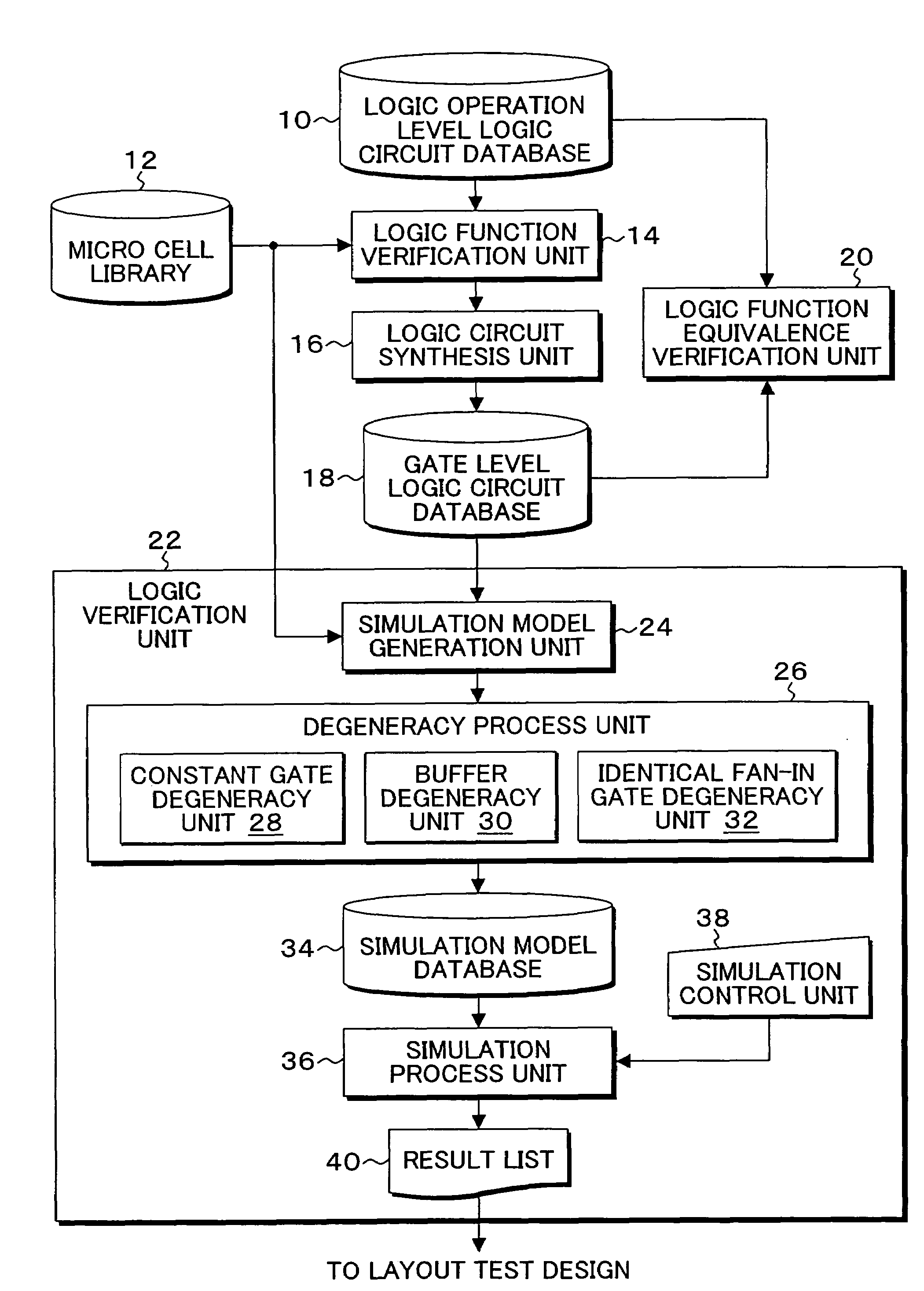
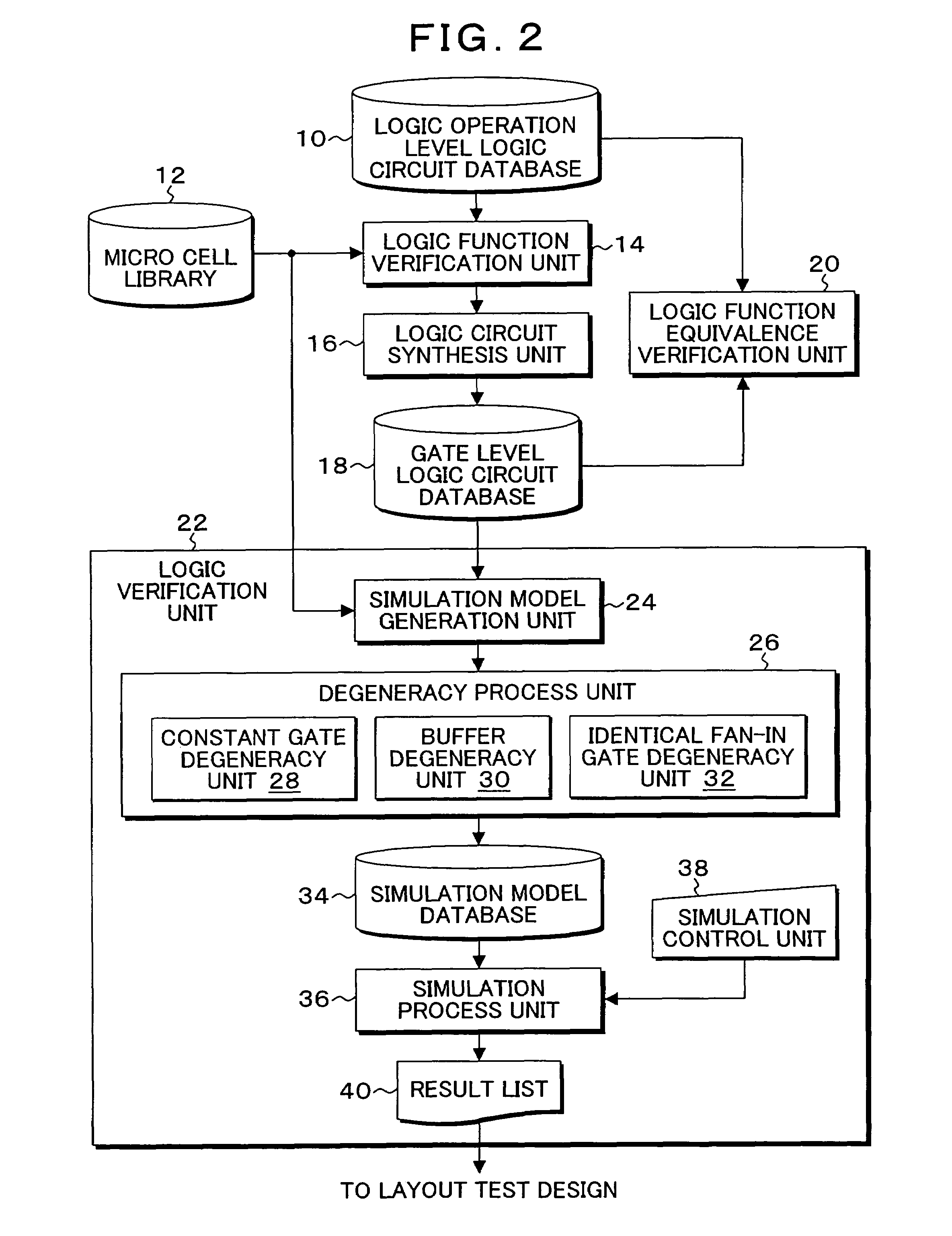
[0046]FIG. 2 is a block diagram of function structures of function design and logic design in a integrated circuit designing system to which the present invention is applied. Normally, in process operations of computer-aided integrated circuit design, firstly as system design, what function blocks the entire system is divided into and how the blocks are operated are determined in order to achieve an intended system usage. Subsequently to this system design, function design is performed for designing a register transfer level (RT level) which determines structures and operations inside the function blocks, and subsequently to the function design, function design is performed for designing logic circuits on the gate level. FIG. 2 shows latter half of the function design in such semiconductor design operations and a subsequent portion of the logic design to which the present invention is applied. First, the latter half of the function design consists of a logic operation level logic ci...


PUM


Abstract

When a simulation model generation unit converts logic on the gate level into a basic primitive which can be executed by a simulator to generate a simulation model, for the basic primitives a degeneracy processing unit determines and deletes a gate which can be deleted and which will not affect the delay stage count. The degeneracy processing unit is provided with a constant gate degeneracy unit which puts a plurality of constant gates together, a buffer degeneracy unit which deletes fan-out-free buffers and an identical fan-in gate degeneracy unit which puts identical fan-in gates together.

Description

[0001]This application is a priority based on prior application No. JP 2004-180941, filed Jun. 18, 2004, in Japan.BACKGROUND OF THE INVENTION[0002]1. Field of the Invention[0003]The present invention relates to an integrated circuit designing system, method and program for designing LSIs with the aid of a computer, and, more particularly, to an integrated circuit designing system, method and program for degenerating the size of simulation models for use in logic verification of the LSIs.[0004]2. Description of the Related Art[0005]Conventionally, in a computer-aided automated designing system of LSIs, design works are performed in conformity with design processes such as system design, function design, logic design, circuit design, layout design, design verification and mask data generation. Among these, function design includes designing a register transfer level (RT level) which determines the structure and operation inside a function block and using a logic simulator for verifica...

Claims


Application Information

Patent Timeline
Patent Type & Authority Patents(United States)
IPC IPC(8): G06F17/50G06G7/62
CPCG06F17/5022G06F30/33
Inventor MOCHIZUKI, TSUYOSHI
Owner FUJITSU LTD
Why Eureka
Try Eureka