Method and apparatus for partitioning an integrated circuit chip

a technology of integrated circuits and partitions, applied in computer aided design, program control, instruments, etc., can solve the problems of increasing difficulty in and increasing the difficulty of manually or automatically partitioning chips into physical partitions, etc., to achieve maximize the sensitivity of linear weight, minimize pin count, optimize the effect of pin coun

Active Publication Date: 2007-08-21
SYNOPSYS INC
View PDF17 Cites 11 Cited by
  • Summary
  • Abstract
  • Description
  • Claims
  • Application Information

AI Technical Summary

Benefits of technology

[0019]In a variation on this embodiment, the system calculates Rent's exponent to facilitate minimizing pin count. Rent's exponent is the logarithm of the pin count divided by the logarithm of the instance count for a pair of logic modules. Note that a lower Rent's exponent indicates a lower pin count.
[0020]In a variation on this embodiment, the system calculates the sensitivity of the joint-utilization ratio and the sensitivity of Rent's exponent. The system then calculates the linear combination of the sensitivity of the joint-utilization ratio and the sensitivity of Rent's exponent. Finally, the system maximizes the sensitivity of the linear weight. A tunable parameter can be used to scale the sensitivity of the joint-utilization ratio relative to the sensitivity of Rent's exponent, thereby facilitating a trade-off between optimizing timing and optimizing pin count.

Problems solved by technology

However, as integrated circuit (IC) designers integrate more system components onto a single chip, IC designs are reaching and exceeding the limits of the IC design tools, specifically the logic optimization and detailed place-and-route tools.
As chip designs become larger, the task of manually or automatically partitioning a chip into physical partitions, while accounting for timing and pin count constraints, becomes progressively more difficult.
Cells belonging to different physical partitions are placed, optimized, and routed within their own disjoint layout areas, which can result in inter-block wires that are longer than intra-block wires.
Since wire delay dominates the overall chip delay, these longer intra-block wires can have an adverse effect on circuit timing.
As a result, the placement and routing in each partition is optimized, but the placement and routing between the partitions is not optimized.
Since each partition was placed and routed separately, wire 126, which connects cells 112 and 116 is relatively long, which may cause timing problems.

Method used


Image

  • Method and apparatus for partitioning an integrated circuit chip
  • Method and apparatus for partitioning an integrated circuit chip
  • Method and apparatus for partitioning an integrated circuit chip

Examples


Embodiment Construction

[0032]The following description is presented to enable any person skilled in the art to make and use the invention, and is provided in the context of a particular application and its requirements. Various modifications to the disclosed embodiments will be readily apparent to those skilled in the art, and the general principles defined herein may be applied to other embodiments and applications without departing from the spirit and scope of the present invention. Thus, the present invention is not limited to the embodiments shown, but is to be accorded the widest scope consistent with the principles and features disclosed herein.

Placement-Based Partitioning

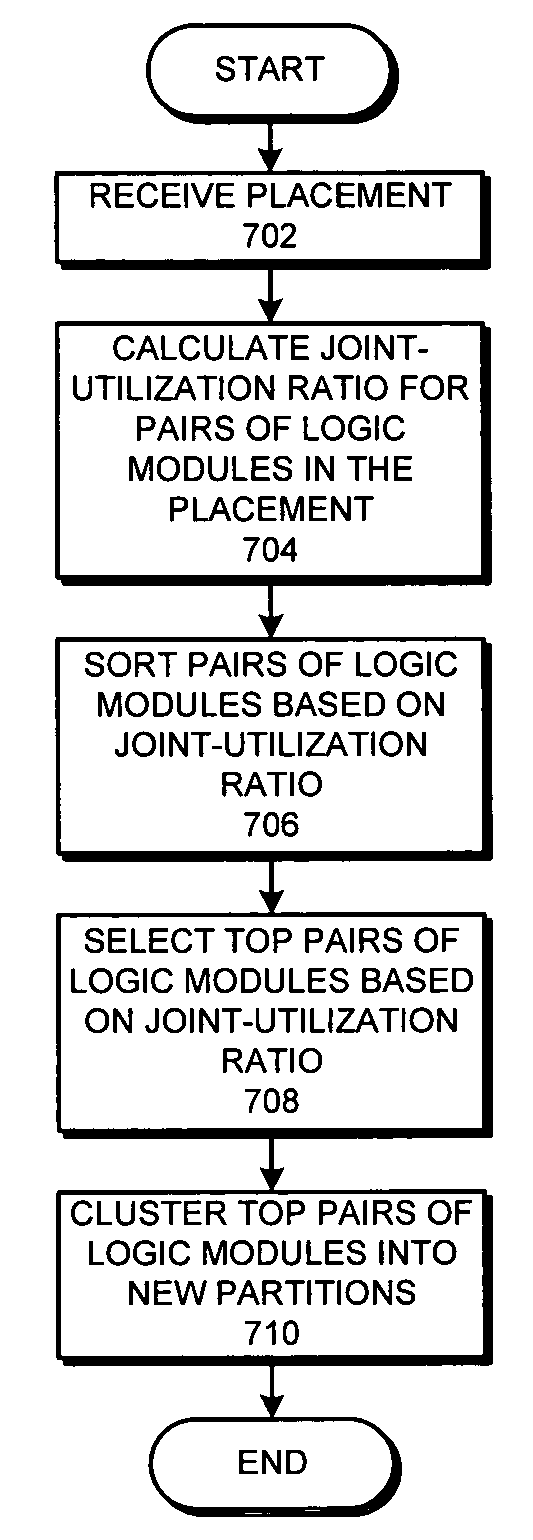
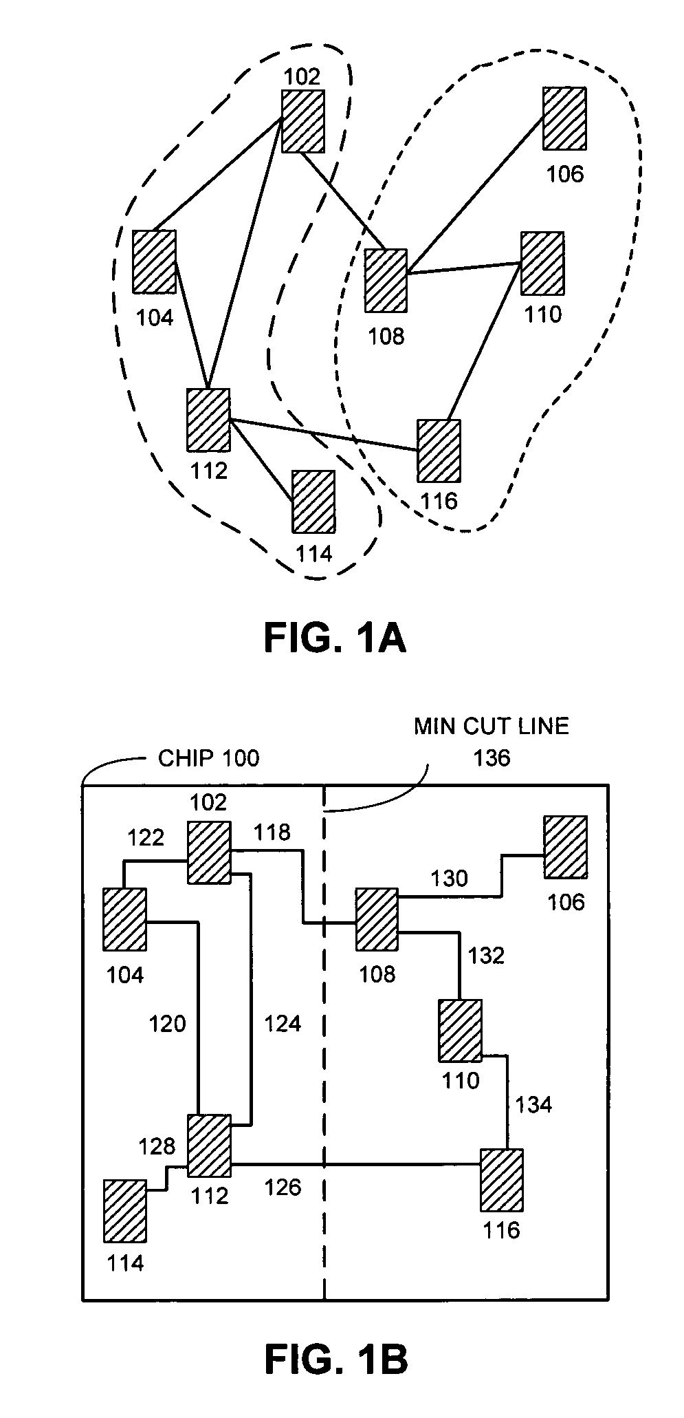
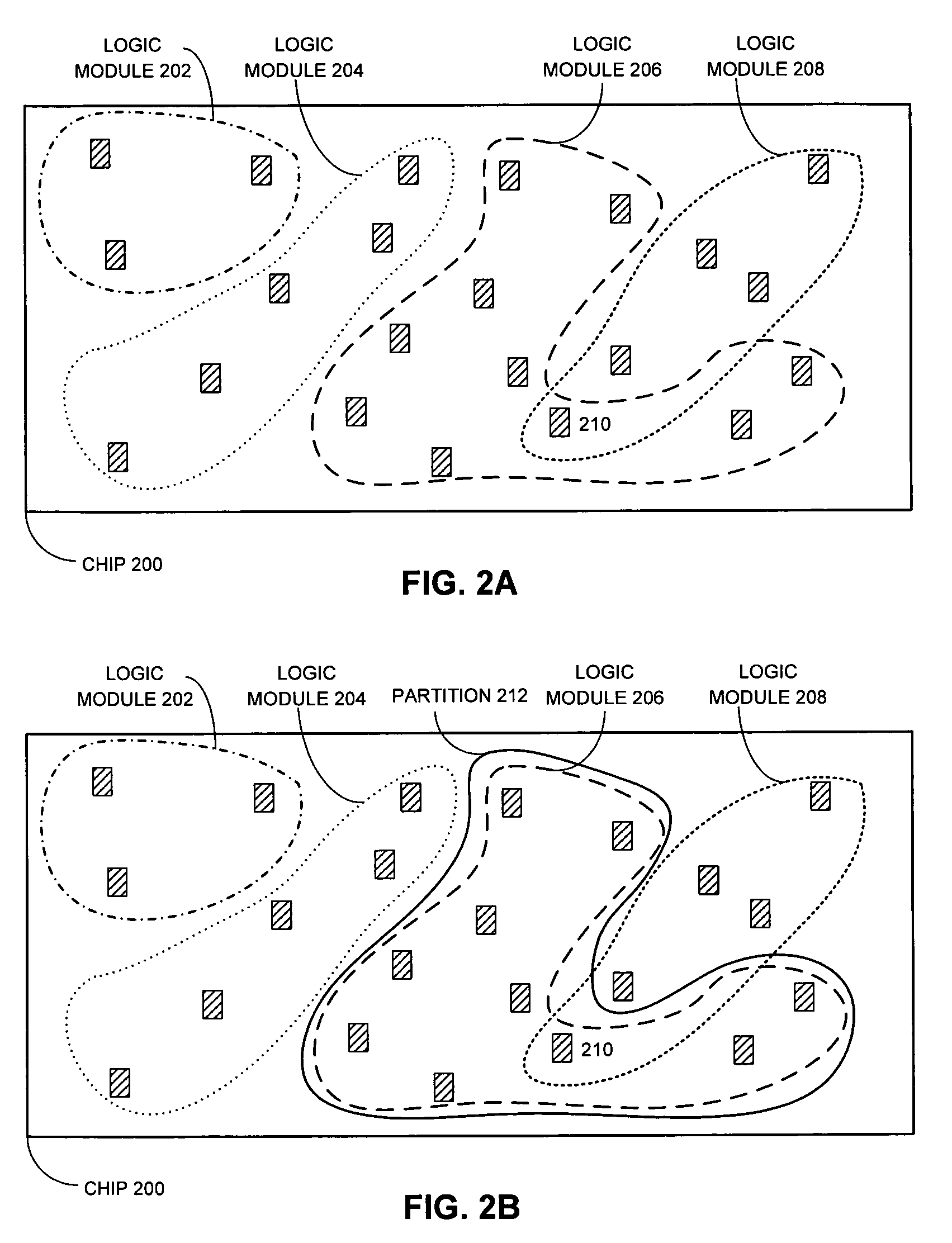
[0033]The present invention automatically partitions a chip using a flat placement. In one embodiment of the present invention, the system uses a timing-driven placement technique. A timing-driven placement technique places cells to optimize timing. In another embodiment of the present invention, the system uses a power-driven plac...


PUM


Abstract

A system that partitions an integrated circuit. First, the system receives a placement for an integrated circuit. The system then calculates a joint-utilization ratio for pairs of logic modules in the placement. Next, the system sorts the pairs of logic modules based on the joint-utilization ratio. The system then selects top pairs of logic modules based on the joint-utilization ratio and clusters the top pairs of logic modules into new partitions.

Description

RELATED APPLICATION[0001]This application hereby claims priority under 35 U.S.C. § 119 to U.S. Provisional Patent Application No. 60 / 626,048 filed 8 Nov. 2004, entitled “Placement Based Design Partitioning,” by inventors Pei-Hsin Ho and Yongseok Cheon.BACKGROUND[0002]1. Field of the Invention[0003]The present invention relates to techniques for partitioning the design of an integrated circuit (IC) chip into smaller design blocks.[0004]2. Related Art[0005]Advances in semiconductor technology presently make it possible to integrate large-scale systems, including tens of millions of transistors, onto a single semiconductor chip. Integrating such large-scale systems onto a single semiconductor chip increases the speed at which such systems can operate, because signals between system components do not have to cross chip boundaries, and are not subject to lengthy chip-to-chip propagation delays. Moreover, integrating large-scale systems onto a single semiconductor chip significantly reduc...

Claims


Application Information

Patent Timeline
Patent Type & Authority Patents(United States)
IPC IPC(8): G06F17/50
CPCG06F17/5072G06F2217/78G06F30/392G06F2119/06
Inventor HO, PEI-HSINCHEON, YONGSEOK
Owner SYNOPSYS INC
Why Eureka
Try Eureka