
Intermediate product manufacturing apparatus, and manufacturing method

Inactive Publication Date: 2007-08-28
SEIKO EPSON CORP
View PDF13 Cites 3 Cited by
  • Summary
  • Abstract
  • Description
  • Claims
  • Application Information

AI Technical Summary

Benefits of technology

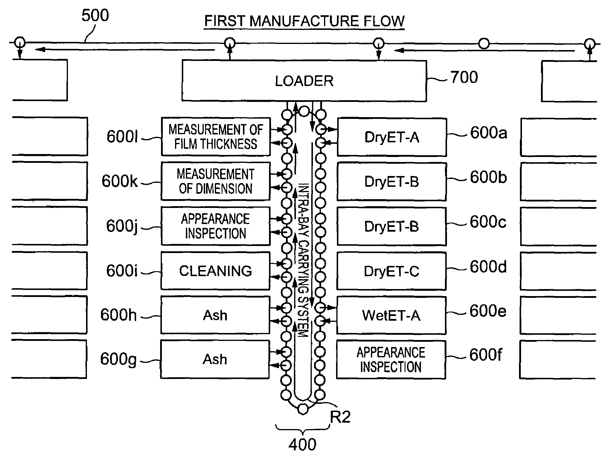
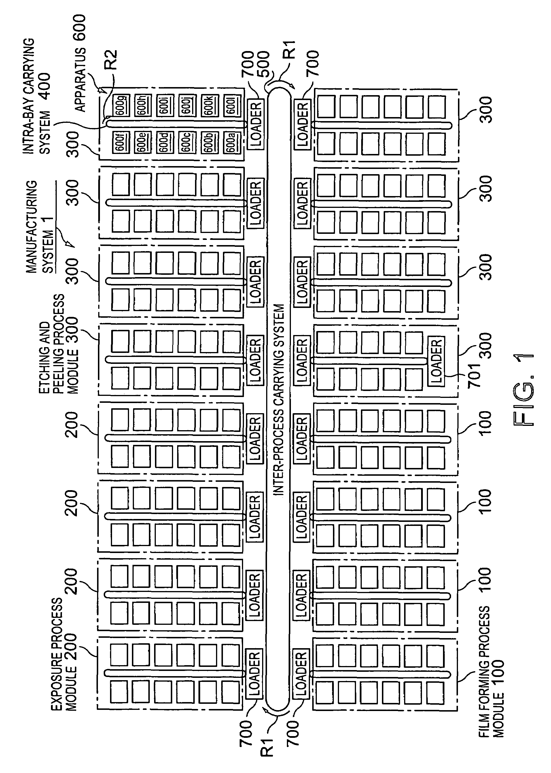
[0011]According to the above construction, by using a container capable of storing a plurality of intermediate products as a unit, the containers are carried between the process modules, and the intermediate products are removed from the containers in each process module. Then, the intermediate products are carried within each process module in a single product state. The plurality of processing means are arranged substantially in the carrying direction of the intermediate products in accordance with the order of processes to be performed on the intermediate products, without arranging the plurality of processing means for performing the same kinds of processes on the intermediate products in a group. For this reason, when the intermediate products are carried in the carrying direction, the plurality of processing means can efficiently perform the plurality of processes, respectively. Therefore, it is not necessary to repeatedly circulate the intermediate products within the process modules as in the conventional art, and for example, through one circulation, the intermediate products are efficiently subjected to a series of continuous processes. In each process module, since the intermediate products are carried in a single product state, not in a container unit, it is possible to manufacture a variety of intermediate products in small quantities.
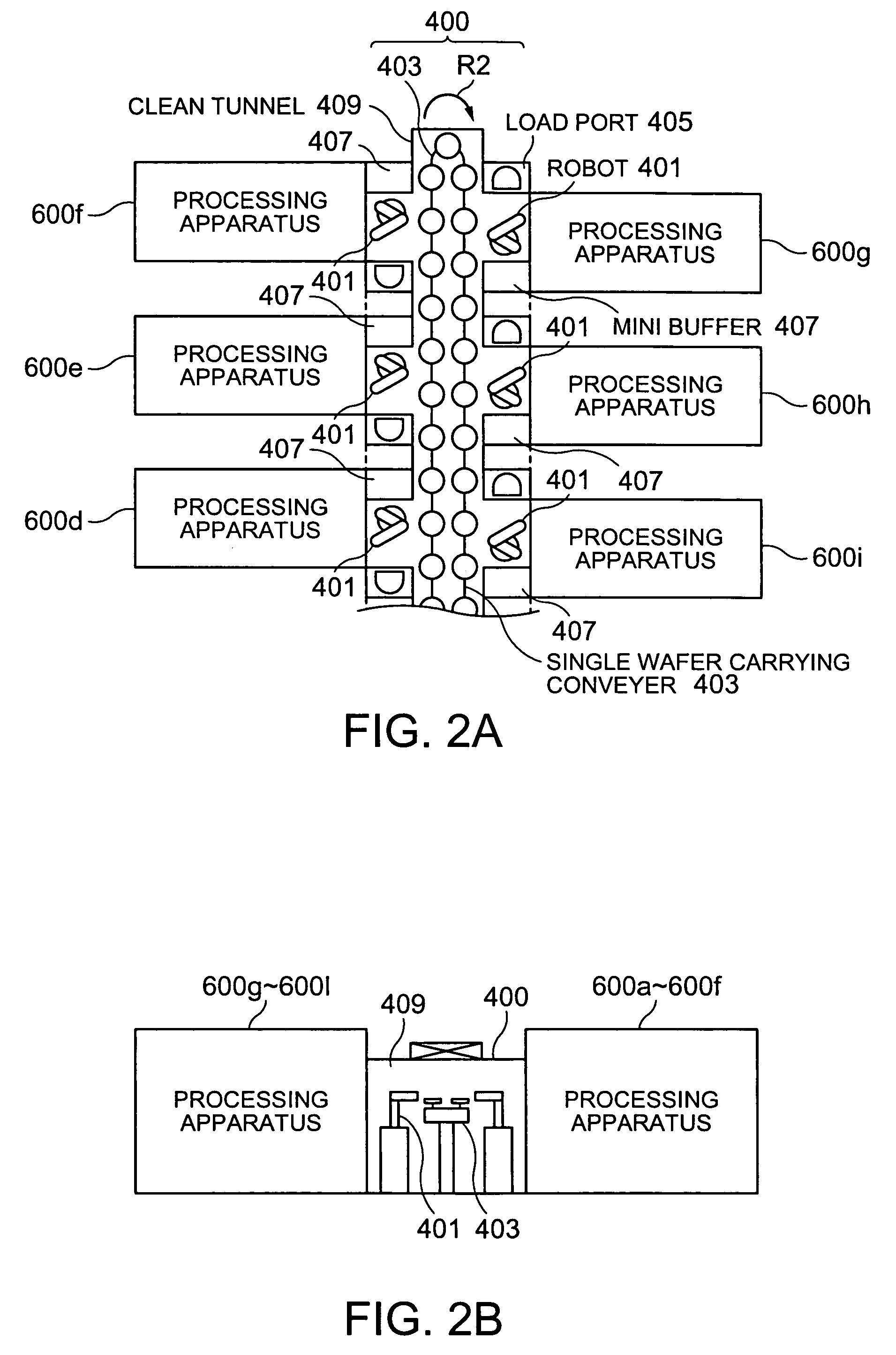
[0013]According to the above construction, the intermediate products can be temporarily stored, corresponding to the carrying situation of the intermediate products between the process modules by the inter-process carrying means or to the carrying situation of the intermediate products within the process modules by the intra-process carrying means. Therefore, the transfer means can efficiently transfer the intermediate products between the inter-process carrying means and the intra-process carrying means, corresponding to the carrying situation of the intermediate products being carried.
[0015]According to the above construction, since the plurality of intermediate products to be processed in the same next process module are stored in a bundle in the same container and are then carried between the process modules, it is possible to more efficiently carry the intermediate products, compared with cases in which the plurality of intermediate products to be processed in different next process modules are mixed and then the intermediate products are carried between the process modules. Furthermore, according to the above construction, since it is possible to minimize the wait time when the maximum number of intermediate products capable of being stored in the container is reached and then the intermediate products are carried in a container unit, that is, the wait time for completion of processes on other intermediate products to be stored in the same container, it is possible to considerably reduce the lead time, compared with the conventional case.
[0017]According to the above construction, it is not necessary to repeatedly circulate the plate-shaped intermediate products within the process modules as in the conventional case, and, for example, through only one circulation, it is possible to efficiently perform a series of continuous processes thereon. Accordingly, since the carrying time of the plate-shaped intermediate products is shortened, particles are hardly attached to the plate-shaped intermediate products. Furthermore, since the carrying time is shortened, it is also possible to considerably reduce the lead time.
[0019]According to the above construction, it is not necessary to repeatedly circulate the semiconductor wafers within the process modules as in the conventional case, and, for example, through only one circulation, it is possible to efficiently perform a series of continuous processes thereon. Accordingly, since the carrying time of the semiconductor wafers is shortened, particles are hardly attached to the semiconductor wafers. Furthermore, since the carrying time is shortened, it is also possible to considerably reduce the lead time.
[0021]According to the above construction, it is not necessary to repeatedly circulate the substrates for liquid crystal display devices within the process modules as in the conventional case, and, for example, through only one circulation, it is possible to efficiently perform a series of continuous processes thereon. Accordingly, since the carrying time of the substrates for the liquid crystal display devices is shortened, particles are not attached well to the substrates for liquid crystal display devices. Furthermore, since the carrying time is shortened, it is also possible to considerably reduce the lead time.

Problems solved by technology

The job-shop has an advantage in that it is easy to maintain and manage the processing apparatuses, but also has a disadvantage in that it takes a long period of time to carry the semiconductor wafers between the processing apparatuses.
That is, when all of the processes are performed using the flow-shop scheme, there are problems in that the processing speed for all of the processes is lowered in accordance with a processing apparatus with a low processing speed.
On the contrary, for example, while only one processing apparatus with a high processing speed may be required for the job-shop, a plurality of the processing apparatuses may be required for the flow-shop, necessitating an increased investment cost.
Accordingly, since the carrying time of the substrates for the liquid crystal display devices is shortened, particles are not attached well to the substrates for liquid crystal display devices.

Method used


Image

  • Intermediate product manufacturing apparatus, and manufacturing method
  • Intermediate product manufacturing apparatus, and manufacturing method
  • Intermediate product manufacturing apparatus, and manufacturing method

Examples


second embodiment

[0084]In a manufacturing apparatus and a manufacturing method according to a second embodiment of the present invention, elements indicated by the same reference numerals as those in FIGS. 1 to 10 have substantially the same constructions, the same reference numerals as those in FIGS. 1 to 10 are used for the same constructions. Therefore, the description thereof will be omitted, and the following description will be focused on different points.

[0085]The second embodiment is characterized in that the inter-process carrying system 500 carries a cassette even before the maximum number of semiconductor wafers capable of being stored in the cassette is reached. Here, the intra-process carrying system 400 may select a plurality of semiconductor wafers to be processed in the same next process module, store the selected semiconductor wafers in the cassette in a bundle, and then transfer the cassette to the inter-process carrying system 500. That is, the plurality of semiconductor wafers to...


PUM


Abstract

A manufacturing apparatus is provided comprising: inter-process carrying means for carrying a container between the process modules in a container unit, the container being capable of storing a plurality of intermediate products therein; intra-process carrying means for removing the intermediate products from the container and carrying the intermediate products within each process module in a single product state; and a plurality of processing means for performing the plurality of processes, respectively, within each process module, wherein the plurality of processing means are arranged substantially in the carrying direction of the intermediate products in accordance with the order of processes to be performed on the intermediate products, without arranging a plurality of processing means for performing the same kinds of processes on the intermediate products in a group.

Description

RELATED APPLICATIONS[0001]This application claims priority to Japanese Patent Application Nos. 2003-100522 filed Apr. 3, 2003 and 2003-190569 filed Jul. 2, 2003 which are expressly incorporated by reference herein in their entireties.BACKGROUND[0002]1. Technical Field of the Invention[0003]The present invention relates to a manufacturing apparatus and a manufacturing method for manufacturing an intermediate product via process modules for performing a plurality of processes.[0004]2. Description of the Related Art[0005]Conventionally, substrates for liquid crystal display devices are manufactured, for example, by using processes for manufacturing semiconductor wafers. The conventional processes for manufacturing semiconductor wafers mainly include wafer manufacturing processes, wafer processing processes, assembly processes, and inspection processes. In the wafer processing processes, which are also called preprocess, a plurality of processes are repeatedly performed on the semicondu...

Claims


Application Information

Patent Timeline
IPC IPC(8): H01L21/00H01L21/64B65G49/06B65G49/07H01L21/02H01L21/677H01L21/68
CPCH01L21/67276Y10T29/41F24D5/005F24D12/02F24D19/0087F24D2200/14
Inventor TANAKA, SHUJIKOBAYASHI, YOSHITAKEFUJIMURA, HISASHI
Owner SEIKO EPSON CORP
Learn More