Chip package structure

a technology of chip and package, applied in the direction of printed circuit aspects, sustainable manufacturing/processing, final product manufacturing, etc., can solve the problems of thermal stress failure of the chip package b>40/b>, cracks may propagate inside the bump, and the reliability of the electrical connection between the chip and the carrier is compromised, so as to reduce fatigue failure

Active Publication Date: 2007-08-28
ADVANCED SEMICON ENG INC
View PDF20 Cites 7 Cited by
  • Summary
  • Abstract
  • Description
  • Claims
  • Application Information

AI Technical Summary

Benefits of technology

[0010]Accordingly, at least one objective of the present invention is to provide a chip packaging process capable of reducing fatigue failure due to a difference in coefficient of thermal expansion between various materials constituting the chip package.
[0011]At least a second objective of the present invention is to provide a chip package structure capable of reducing fatigue failure due to a difference in coefficient of thermal expansion between various materials constituting the chip package.
[0016]Accordingly, the chip packaging process of the present invention includes the step of forming a plurality of supporting structures around the junctions between the bumps and the carrier. Thus, the bumps can have a higher tolerance for thermal stress and the electrical connection between the chip and the carrier can have a greater reliability. Ultimately, the number of contacts between a chip and a carrier can be increased to produce a chip package with a higher packing density.

Problems solved by technology

However, due to the difference in coefficient of thermal expansion (CTE) between the chip 50, the bumps 60, the underfill layer 70 and the carrier 80, the chip package 40 is vulnerable to thermal stress failure resulting from cyclic temperature variations due to repeated operation.
Since cyclic stress in these areas can cause fatigue, cracks may propagate inside the bumps.
Ultimately, the reliability of the electrical connection between the chip and the carrier will be compromised.
Furthermore, increasing the area of contact between the bumps and the contacts will lower the average height of the bumps and subject the bumps to a higher thermal stress.

Method used


Image

  • Chip package structure
  • Chip package structure
  • Chip package structure

Examples


Embodiment Construction

[0021]Reference will now be made in detail to the present preferred embodiments of the invention, examples of which are illustrated in the accompanying drawings. Wherever possible, the same reference numbers are used in the drawings and the description to refer to the same or like parts.

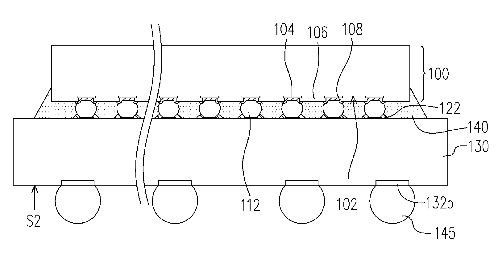
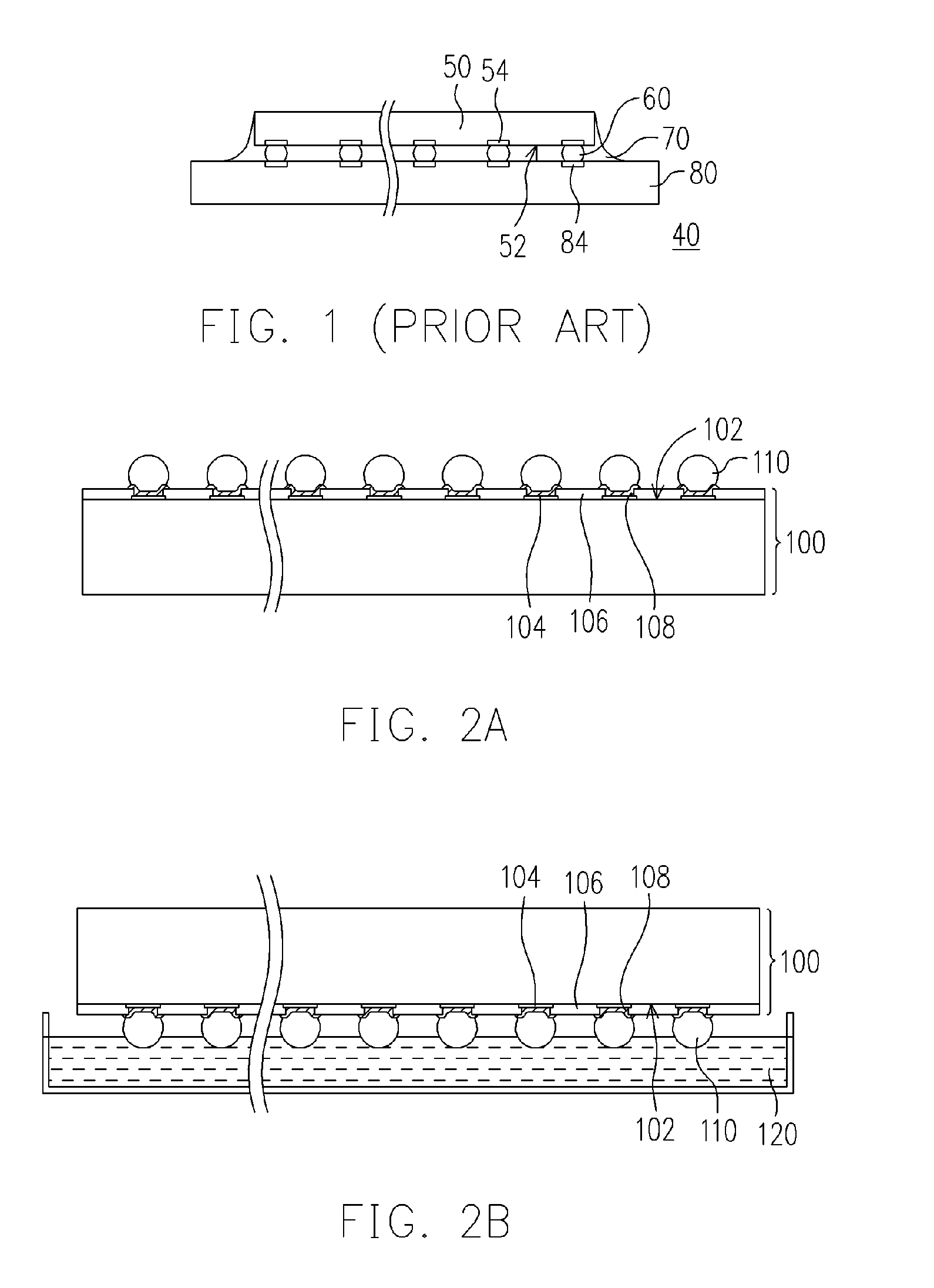
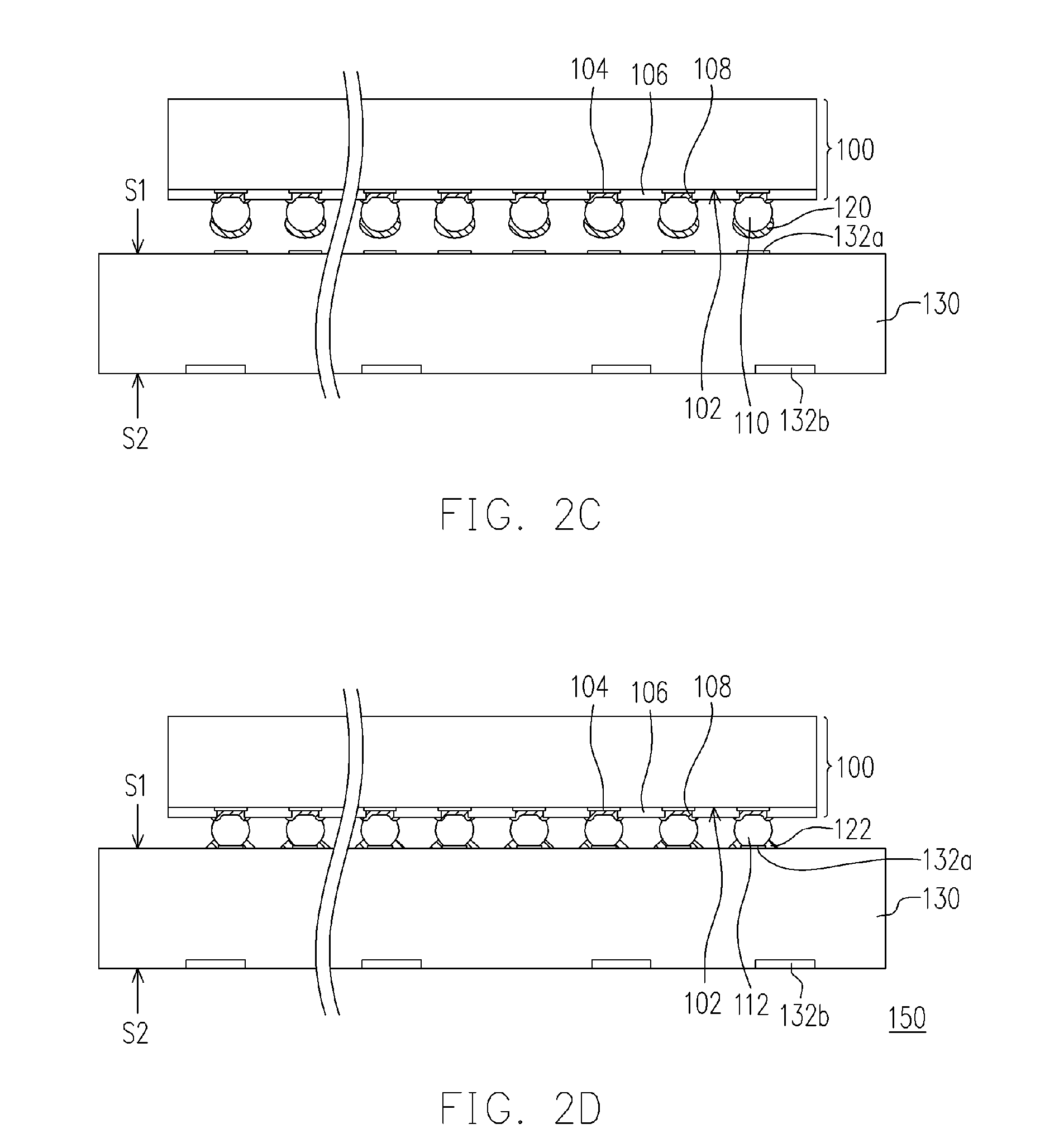
[0022]FIGS. 2A through 2F are schematic cross-sectional views showing the steps for producing a chip package according to one preferred embodiment of the present invention. As shown in FIG. 2A, a chip 100 having an active surface 102 is provided. The active surface 102 has a plurality of solder bumps 110 disposed thereon. The active surface 102 of the chip 100 also includes a plurality of bonding pads 104 and a passivation layer 106. The passivation layer 106 protects the chip 100 but exposes the bonding pads 104. The solder bumps 110 are disposed on the bonding pads 104. Furthermore, an under bump metallurgy (UMB) 108 is also disposed between each bonding pad 104 and a corresponding solder bump 110....


PUM


Abstract

A process for fabricating a chip package structure with the following steps is provided. First, a chip having an active surface is provided. A plurality of solder bumps is disposed on the active surface. Then, a polymer material including flux is placed on the surface of the solder bumps by a dipping process. The chip is disposed on a carrier such that the carrier is in contact with the solder bumps. A reflow process is carried out so that the chip and the carrier are electrically connected through the solder bumps and a plurality of supporting structures made from the polymer material are formed around the junctions between the solder bumps and the carrier. The supporting structures enhance the endurance of the solder bumps to thermal stress and reduce damage due to fatigue.

Description

CROSS-REFERENCE TO RELATED APPLICATION[0001]This application claims the priority benefit of Taiwan application serial no. 93122841, filed on Jul. 30, 2004. All disclosure of the Taiwan application is incorporated herein by reference.BACKGROUND OF THE INVENTION[0002]1. Field of the Invention[0003]The present invention relates to a chip package structure and fabricating method thereof. More particularly, the present invention relates to a flip chip bonded chip package structure and process for fabricating the same.[0004]2. Description of the Related Art[0005]As the need for communication is increasingly important in our society, the market for various types of electronic devices expands rapidly. To prepare for the upcoming trend, chip packages often have a design that reflects our need for a digital network connection and more personalized electronic equipment. One way of meeting our demands is to produce highly integrated digital devices having higher processing speed and more powerf...

Claims


Application Information

Patent Timeline
Patent Type & Authority Patents(United States)
IPC IPC(8): H01L23/02H01L23/48H01L29/40H01L21/56H01L21/60H01L23/498H05K3/34
CPCH01L21/563H01L24/11H01L24/81H05K3/3436H01L24/29H01L23/49816H01L2224/13099H01L2224/13111H01L2224/13144H01L2224/16225H01L2224/73203H01L2224/73204H01L2224/81801H01L2224/83191H01L2924/01005H01L2924/0105H01L2924/01075H01L2924/01079H01L2924/01082H01L2924/01327H01L2924/15311H05K3/3489H05K2201/10674H05K2201/10977H01L2924/01006H01L2924/01033H01L2924/014H01L2224/32225H01L2924/00H01L2224/11822H01L2924/3512H01L2924/00013H01L2224/29099H01L2924/351H01L2224/1369H01L2224/13116H01L2224/1357H01L2224/8192H01L2224/81355H01L2224/05022H01L2224/0557H01L2224/05573H01L2224/05001H01L2224/05572H01L2224/056H01L2924/00014H01L2224/05571H01L2224/81011Y02P70/50H01L2224/05099
Inventor CHUNG, CHIH-MING
Owner ADVANCED SEMICON ENG INC
Why Eureka
Try Eureka