Semiconductor device and method of its manufacture

a technology of semiconductors and semiconductors, applied in the direction of semiconductor/solid-state device manufacturing, semiconductor devices, semiconductor devices, etc., can solve the problems of device shorting through easy leakage to the lower contact region, and difficult control of penetration, etc., to achieve the effect of improving efficiency

Inactive Publication Date: 2007-09-11
KK TOSHIBA
View PDF5 Cites 2 Cited by
  • Summary
  • Abstract
  • Description
  • Claims
  • Application Information

AI Technical Summary

Benefits of technology

[0013]In a preferred embodiment, the device further comprises an upper etch stop layer, said upper etch stop layer being provided between said lower conducting region and the active layer, said lower conducting region comprising a first material and said upper etch stop layer comprising a second material, wherein said first material is etchable by a first etchant but resistant to a second etchant and said second material is etchable by the second etchant but resistant to etching by the first etchant. The provision of this upper etch stop layer allows the lower conducting layer to be etched laterally without the etch undercutting the active region. This upper etch stop layer may be purposely engineered into the structure or in some cases, exploited the use an integral layer that is native to the structure e.g. doped Al0.33Ga0.67As region in an inverted high electron mobility transistor (HEMT). Also, this etch stop layer can be a superlattice matrix of the etch stop (e.g. AlAs) and back gate material (e.g. GaAs).
[0014]The semiconductor device further preferably comprises a lower etch stop layer, said lower etch stop layer being provided on the opposing side of said lower conducting region to said active layer, wherein said lower conducting region comprises a first material and said lower etch stop layer comprises a second material, wherein said first material is etchable by a first etchant but resistant to a second etchant and said second material is etchable by the second etchant but resistant to etching by the first etchant. The provision of the lower etch stop layer allows any lateral etching to progress more efficiently since the etch cannot significantly progress downwards due to the lower etch stop layer.
[0016]Generally, a contact will be made to said lower conducting region and wherein said contact to said lower conducting region is provided in a first lateral part of said device and the source or drain contact is formed in a second lateral part of said device, wherein said lower conducting region is removed in an area between said first and second lateral parts such that first and second parts of said lower conducting region are isolated from one another. This complete removal of the lower conducting layer considerably reduces leakage from the source and drain ohmic contacts via the lower conducting layer.

Problems solved by technology

If the further conductive layer or region is a semiconductor layer or region within the device, there is a problem in that the source and drain contacts can also connect to the contact region thus causing the device to short through the lower contact region.
These contacts have the problem in that their penetration can be difficult to control and even if it if correctly controlled they still have a tendency to leak to the lower contact region.
To minimise the problems of the contacts leaking or shorting, a relatively large distance is introduced between the active layer and the lower contact region, thus increasing the size of the device.
In addition, a large operating voltage will be required that inevitably leads to other problems e.g. current leakage and heating.
However, this technique often still require the use of shallow ohmic contacts and hence the associated problems.
Moreover, it is very difficult to align this ohmic contact on the back of the wafer substrate region with the active area of the device on the wafer surface.

Method used


Image

  • Semiconductor device and method of its manufacture
  • Semiconductor device and method of its manufacture
  • Semiconductor device and method of its manufacture

Examples


Embodiment Construction

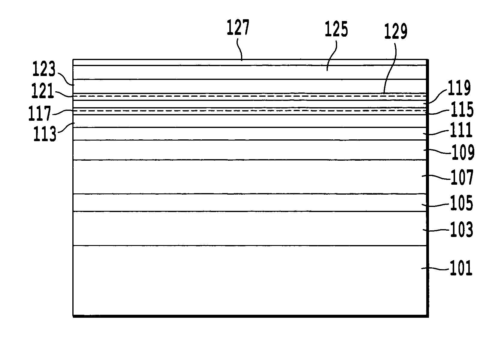
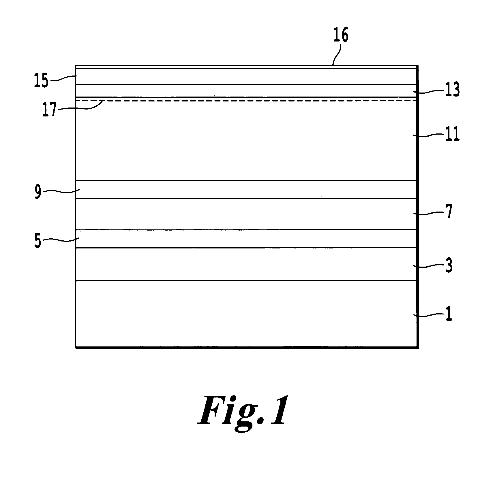
[0037]The layer structure of FIG. 1 comprises a semi-insulating GaAs substrate 1. An insulating GaAs buffer layer 3 is formed overlying and in contact with said substrate. A lower etch stop layer 5 comprising 50 nm AlAs is then formed overlying and in contact with said GaAs buffer layer 3. Lower contact region 7 is then formed overlying and in contact with lower buffer layer 5. Lower contact layer 7 comprises 100 nm of n-doped GaAs. Upper etch stop layer 9 is then formed overlying and in contact with the lower contact layer 7. Upper etch stop layer 9 comprises 50 nm of insulating AlAs.

[0038]Active layer 11 is provided overlying and in contact with upper etch stop layer 9. Active layer 11 comprises 250 nm of insulating GaAs. Spacer layer 13 is then provided overlying and in contact with active layer 11. Spacer layer 13 comprises 40 nm of undoped Al0.33Ga0.67As. Doped barrier layer 15 is then provided overlying and in contact with spacer layer 13. Doped barrier layer 15 comprises 40 n...


PUM


Abstract

A semiconductor device comprising a vertical stack of layers, comprising:an active layer configured to support a two dimensional carrier gas having an excess of carriers;source and drain contacts provided to said active layer such that a current can flow between said source and drain contacts through said two dimensional carrier gas;a lower conducting region,wherein said lower contact conducting region is a patterned lower conducting region such that said active layer is suspended across gaps in said lower conducting region and said active layer is physically supported by and suspended between parts of said lower conducting region.

Description

BACKGROUND OF THE INVENTION[0001]The present invention relates to the field of semiconductor devices and their manufacture. More specifically, the present invention relates to the field of semiconductor devices which have multiple vertically stacked conducting layers and where contact needs to be made to two or more of these conducting layers.[0002]Nearly all semiconductor devices comprise a plurality of vertically stacked layers. In some devices, for example, a field effect transistor (FET), there is a need to measure transport laterally through an active layer and to modulate this transport by applying a field using a further conductive layer or region within the device. To make contact to the active layer, a source contact and a drain contact are used.[0003]If the further conductive layer or region is a semiconductor layer or region within the device, there is a problem in that the source and drain contacts can also connect to the contact region thus causing the device to short t...

Claims


Application Information

Patent Timeline
Patent Type & Authority Patents(United States)
IPC IPC(8): H01L31/072H01L31/0328H01L31/0336H01L31/109H01L21/00H01L21/335H01L29/06H01L29/417H01L29/423H01L29/778
CPCH01L29/0649H01L29/0692H01L29/41725H01L29/42316H01L29/66462H01L29/7785
Inventor SEE, PATRICK UN SIONGSHIELDS, ANDREW JAMES
Owner KK TOSHIBA
Why Eureka
Try Eureka