Analogue to digital conversion device operable on different sampling clocks

a conversion device and digital technology, applied in analogue/digital conversion, transmission systems, instruments, etc., can solve the problems of difficult to obtain highly precise numerical data from the a/d conversion device, difficult to form each transistor of a desired length, and difficult to shift the delay amount, so as to improve the voltage resolution and achieve the effect of highly precise a/d conversion

a conversion device and digital technology, applied in analogue/digital conversion, transmission systems, instruments, etc., can solve the problems of difficult to obtain highly precise numerical data from the a/d conversion device, difficult to form each transistor of a desired length, and difficult to shift the delay amount, so as to improve the voltage resolution and achieve the effect of highly precise a/d conversion

US7268719B2Inactive Publication Date: 2007-09-11DENSO CORP

Image

  • Analogue to digital conversion device operable on different sampling clocks
  • Analogue to digital conversion device operable on different sampling clocks
  • Analogue to digital conversion device operable on different sampling clocks

Examples


embodiment

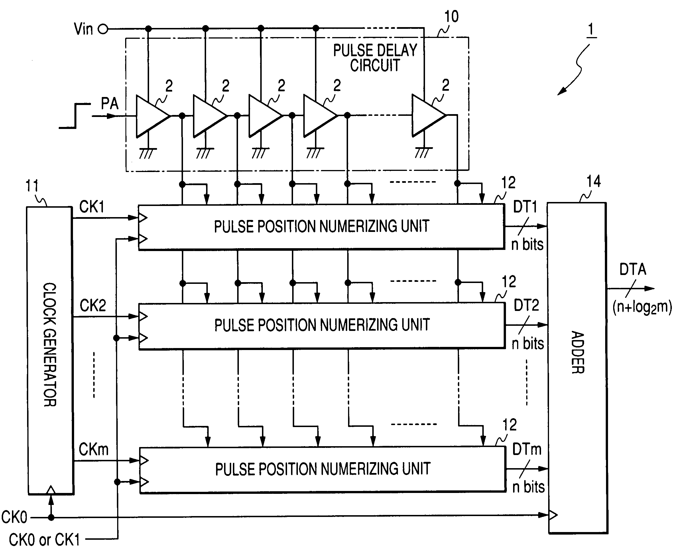
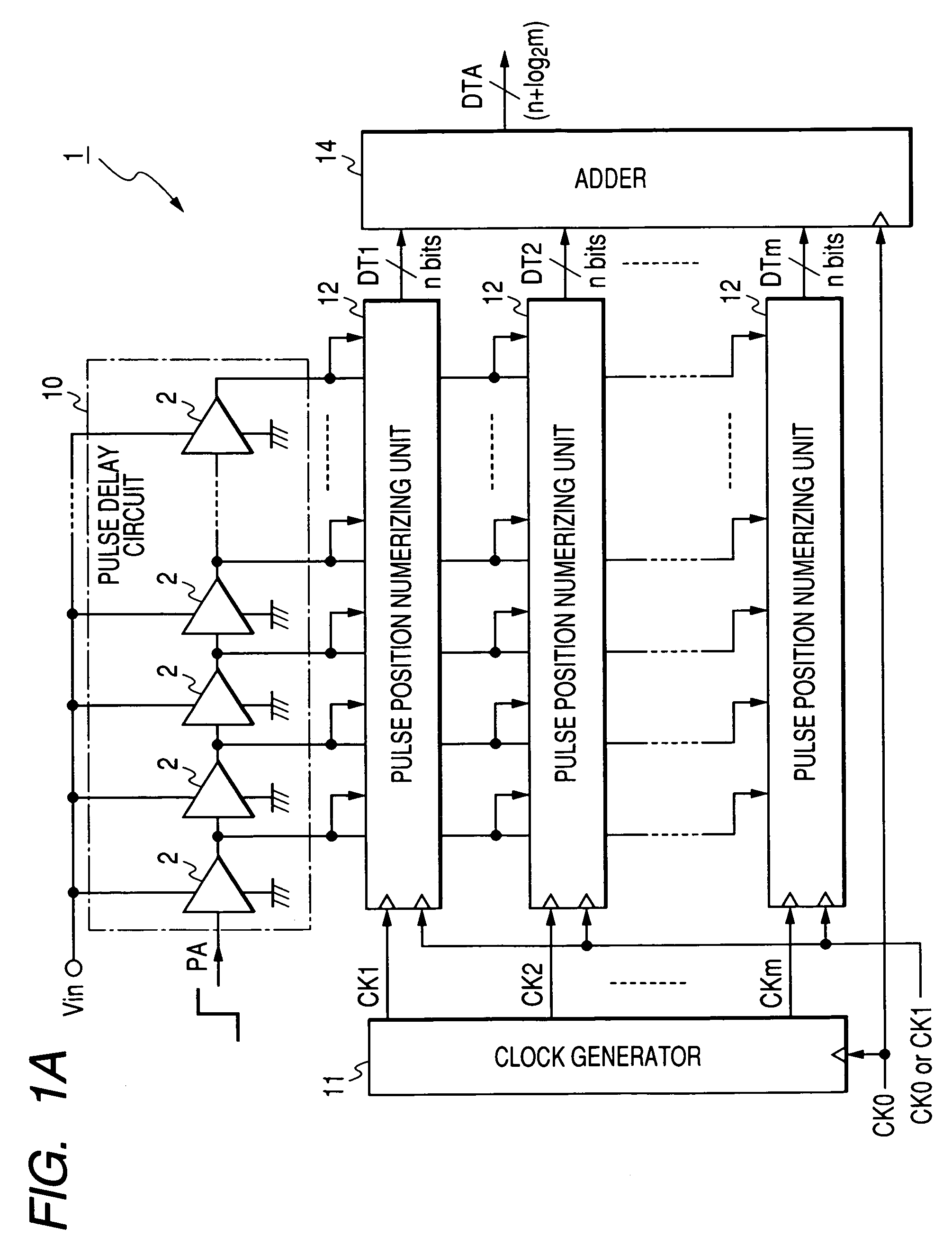
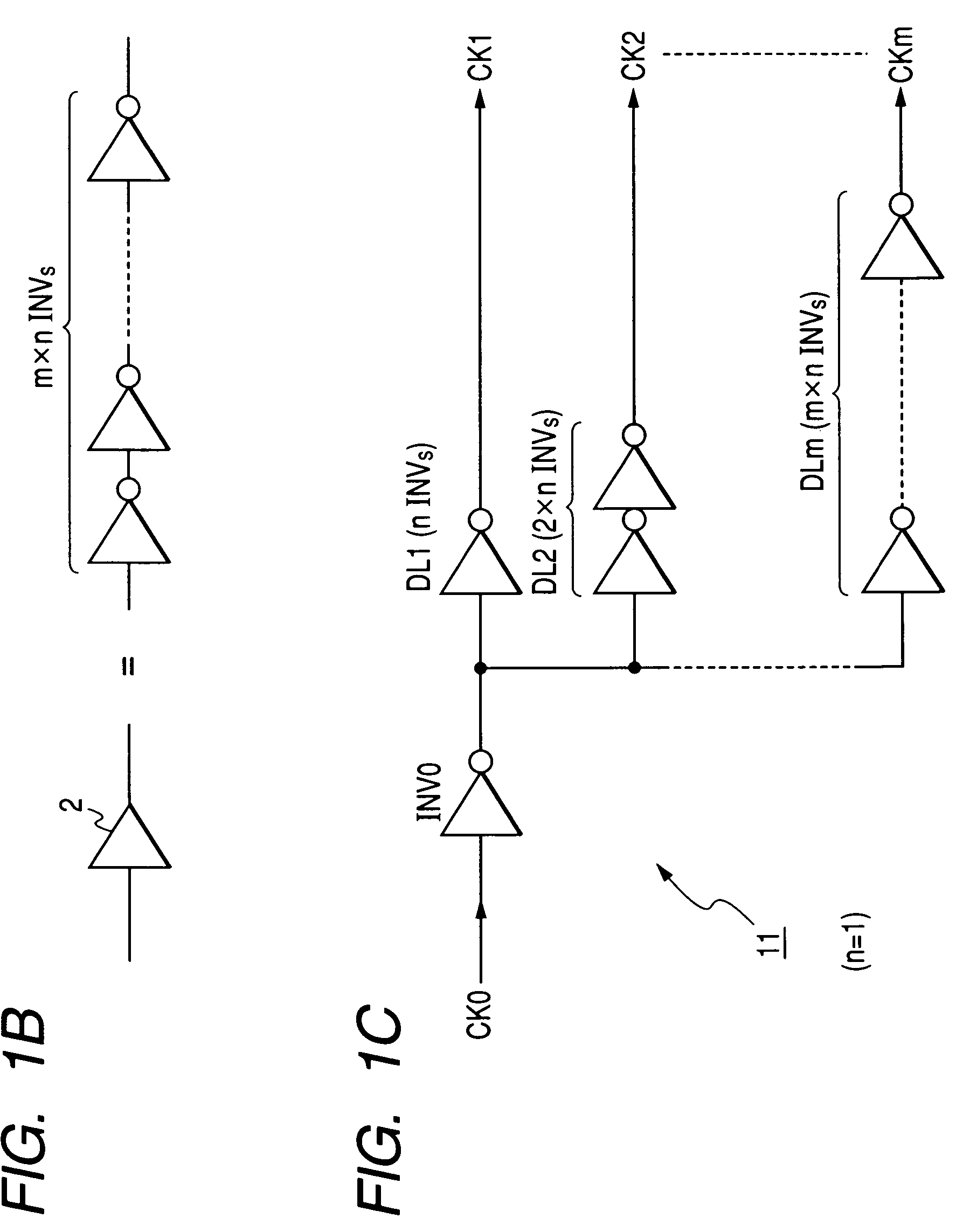
[0034]FIG. 1A is a block diagram showing a configuration of the A / D conversion device 1 according to an embodiment of the present invention. FIG. 1B is an explanatory diagram showing a configuration of the pulse delay circuit 10 incorporated in the A / D conversion circuit 1 shown in FIG. 1A, and FIG. 1C is an explanatory diagram showing a configuration of the clock generator 11 incorporated in the A / D conversion circuit 1 shown in FIG. 1A. Further, FIG. 2A and FIG. 2B are timing charts showing a sampling clock and a sampling time of each pulse position numerizing units 12 incorporated in the A / D conversion circuit 1 shown in FIG. 1A;

[0035]As shown in FIG. 1A, the A / D conversion device 1 of the embodiment has a pulse delay circuit 10, a clock generator 11, “m” pulse position numerizing units 12, and an adder 14. In the A / D conversion device 1, the pulse delay circuit 10 has 2n delay units 2. As shown in FIG. 1B, each delay unit 2 has m×n inverters INV (as inverting circuits, n=1 in th...


PUM


Abstract

In an A / D conversion device, each delay unit in a pulse delay circuit has inverters INV of m×n stages (m, n are positive integers), a clock generator has m-delay lines, and each delay line has inverters INV of i×n stages (i=1, 2, . . . , and m). Those delay lines DL1 to DLm output sampling clocks CK1 to CKm. Each of those inverters INV has a same characteristic. In the A / D conversion device, the delay time in each of the delay lines DL1 to DLm is adjusted by the number of the inverters INV. It is thereby possible to provide the m-sampling clocks CK1 to CKm of a different phase ΔT with one another, namely whose phases are preciously shifted by ΔT with one another.

Description

CROSS-REFERENCE TO RELATED APPLICATIONS[0001]This application is related to and claims priority from Japanese Patent Application No. 2005-132209 filed on Apr. 28, 2005, the contents of which are hereby incorporated by reference.BACKGROUND OF THE INVENTION[0002]1. Field of the Invention[0003]The present invention relates to an analog to digital (A / D) conversion device for converting an analog input signal into numerical data using a pulse delay circuit that has a plurality of delay units connected in series with one another, each of the delay units inputs, delays, and outputs a pulse signal.[0004]2. Description of the Related Art[0005]As shown in FIG. 5A, a pulse delay type A / D conversion device 500 has been known, which has a pulse delay circuit 100, a clock generator 110, “m” pulse position numerizing units 120, and an adder 14. Such a pulse delay type A / D conversion device was disclosed in a Japanese patent laid open publication number JP 2004-7385, for example. In the conventiona...

Claims


Application Information

Patent Timeline
11 Sep 2007
Publication
US7268719B2
IPC
H03M1/60
CPC
G04F10/005; H03M1/502; H03M1/14; H03M1/207; H03M1/60
Inventors
TERAZAWA, TOMOHITO; WATANABE, TAKAMOTO