System and method for mapping logical components to physical locations in an integrated circuit design environment

a technology of integrated circuit design and mapping system, applied in computer aided design, semiconductor/solid-state device details, instruments, etc., can solve the problems of circuits that are difficult to specify (interconnect) correctly, circuits are more difficult to work with, and the behavior of such densely populated integrated circuits is much more subtle and complex

Inactive Publication Date: 2007-09-11
BELL SEMICON LLC
View PDF27 Cites 127 Cited by
  • Summary
  • Abstract
  • Description
  • Claims
  • Application Information

AI Technical Summary

Problems solved by technology

As the number of interconnections have increased, the challenge of translating a circuit designer's intended “specific functionality” into a working IC has also increased, exponentially.
In particular, since complex integrated circuits now contain large numbers of transistors, gates, semiconductors and interconnections, the circuits are more difficult to specify (interconnect) correctly.
Additionally, the laws of physics that govern the behavior of such densely populated integrated circuits are much more subtle and complex than that of larger, less dense chips.
Unanticipated and sometimes subtle interactions between the transistors and other electronic structures may adversely affect the performance of the circuit.
Such issues increase the expense and risk of designing and fabricating integrated circuits.
Manually assigning logical blocks to physical chip locations is a time-consuming, error-prone, and expensive task.
Given that there may be millions of circuit elements on a given chip, this task may be impossible to complete in any reasonable amount of time through manual methods.
None of these tools are capable of handling the complex process rules required for legal placement of cells on specific, pre-manufactured diffused silicon slices.

Method used


Image

  • System and method for mapping logical components to physical locations in an integrated circuit design environment
  • System and method for mapping logical components to physical locations in an integrated circuit design environment
  • System and method for mapping logical components to physical locations in an integrated circuit design environment

Examples


Embodiment Construction

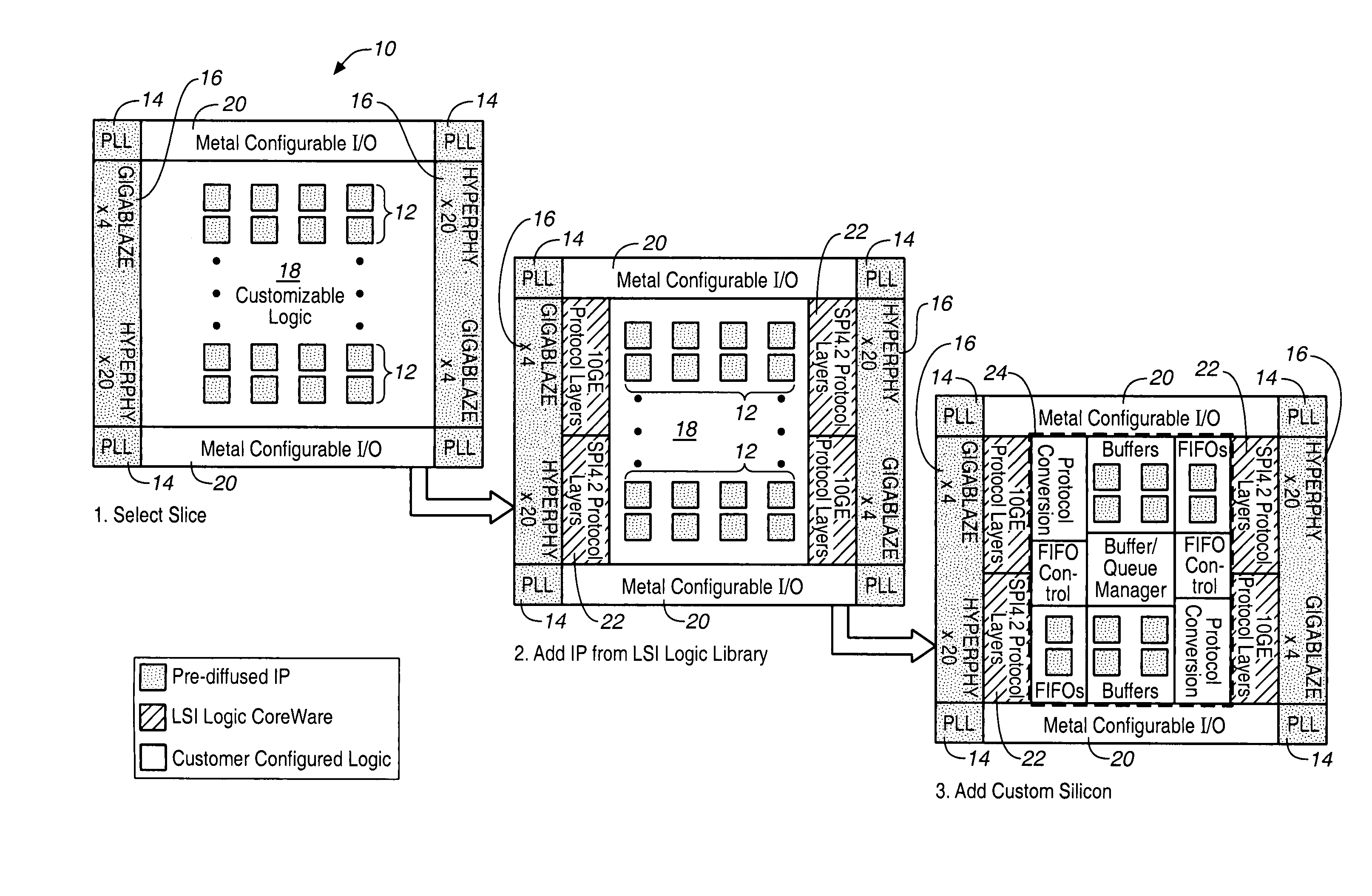
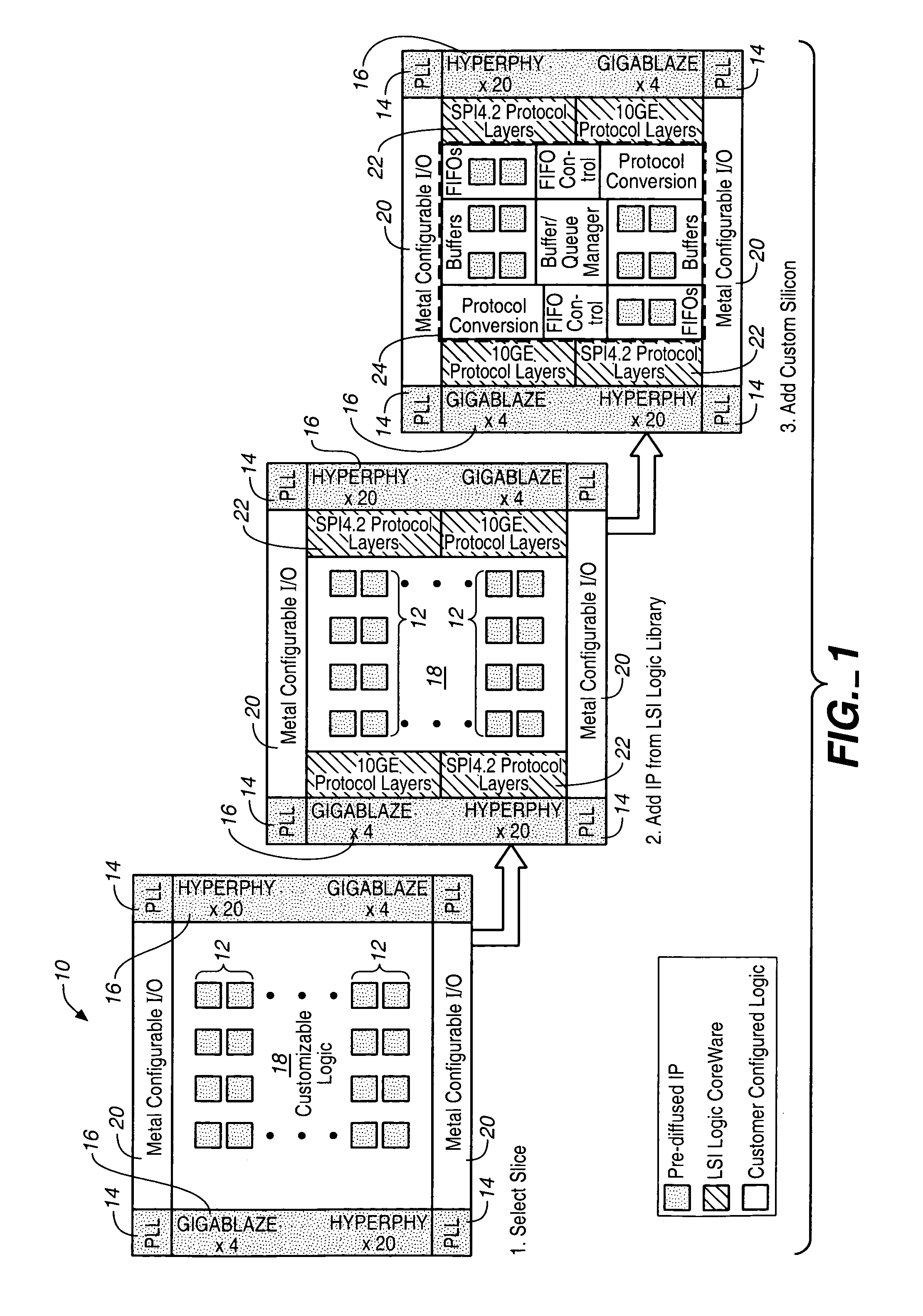
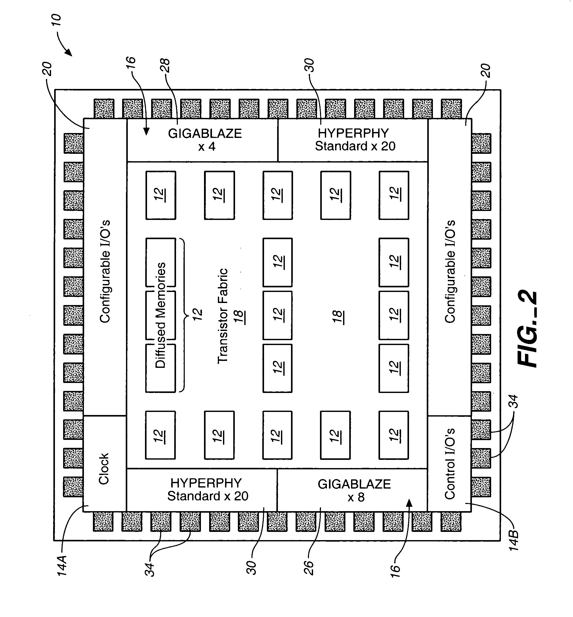
[0027]The present invention relates to a computer aided physical design process of an integrated circuit. For example, embodiments of the present invention are useful with the methods and processes described in U.S. patent application Ser. No. 10 / 335,360, filed on Dec. 31, 2002, and the other patent applications referenced above by serial number in the Cross-Reference to Related Applications, all of which are incorporated herein by reference in their entirety.

[0028]One technique for accelerating the integrated circuit design process involves utilization of existing logical and physical components, which are sometimes referred to as “function blocks” or “Intellectual Property” (IP) blocks. Another technique involves utilizing a prefabricated, unmetallized chip slice as the base layers for the design process, so that standardized Input / Output (I / O) circuitry, clocks, and the like need not be recreated for each integrated circuit in order to complete the circuit design.

[0029]As used he...


PUM


Abstract

A system and method for mapping Intellectual Property (IP) components onto a pre-fabricated chip slice allows a user to select a target location for placement of an IP component onto a slice. A slice definition of the pre-fabricated chip slice is searched for a legal location for the IP component that is near to the target location. The IP component is mapped to the legal location.

Description

CROSS-REFERENCE TO RELATED APPLICATIONS[0001]The present application is related to the following U.S. Patent Applications: U.S. patent application Ser. No. 10 / 435,168, filed May 8, 2003 (U.S. Pat. No. 7,020,852); U.S. patent application Ser. No. 10 / 318,792, filed Dec. 13, 2002; U.S. patent application Ser. No. 10 / 318,623, filed Dec. 13, 2002; U.S. patent application Ser. No. 10 / 334,568, filed Dec. 31, 2002 (U.S. Pat. No. 6,823,502); U.S. patent application Ser. No. 10 / 465,186, filed Jun. 19, 2003 (U.S. Pat. No. 6,959,428); U.S. patent application Ser. No. 10 / 335,360, filed Dec. 31, 2002 (U.S. Pat. No. 7,055,113); U.S. patent application Ser. No. 10 / 664,137, filed Sep. 17, 2003 (U.S. Pat. No. 6,910,201); U.S. patent application Ser. No. 10 / 459,158, filed Jun. 11, 2003 (U.S. Pat. No. 6,871,154); and U.S. patent application Ser. No. 10 / 245,148, filed Sep. 16, 2002 (U.S. Pat. No. 7,017,093), the contents of which are hereby incorporated by reference in their entireties.BACKGROUND OF THE...

Claims


Application Information

Patent Timeline
Patent Type & Authority Patents(United States)
IPC IPC(8): G06F17/50H01L23/544
CPCG06F17/5072G06F30/392
Inventor KHAKZADI, KHOSROTREMEL, CHRIS J.DILLON, MICHAEL N.
Owner BELL SEMICON LLC
Why Eureka
Try Eureka