Transistor integrated circuit apparatus

a technology of integrated circuit and transistor, which is applied in the direction of high-frequency amplifiers, amplifiers with min 3 electrodes or 2 pn junctions, radiation controlled devices, etc., can solve the problems of thermal runaway, part of the transistor, and variable operation of the transistor, so as to prevent thermal runaway of the transistor, reduce noise, and superb rf characteristics

Inactive Publication Date: 2007-10-02
COLLABO INNOVATIONS INC
View PDF3 Cites 3 Cited by
  • Summary
  • Abstract
  • Description
  • Claims
  • Application Information

AI Technical Summary

Benefits of technology

[0017]Therefore, an object of the present invention is to provide a transistor integrated circuit apparatus generating less noise, having superb RF characteristics, and preventing thermal runaway of a transistor included therein.
[0024]A transistor integrated circuit apparatus according to the present invention comprises at least one transistor having a first electrode connected to a common output terminal and a second electrode which is grounded; at least one capacitor having one of two electrodes connected to a base electrode of the transistor and the other electrode connected to a common RF signal input terminal; and at least one inductor having one of two electrodes connected to the base of the transistor and the other electrode connected to a DC power supply input terminal. Owing to this configuration, RF noise generated in a DC power supply circuit can be reduced by the inductor, and thus the RF noise output from the transistor can be reduced. The inductor prevents an RF signal input from the RF signal input terminal from flowing toward the DC power supply circuit. Thus, the RF signal can be prevented from being lost by the flow thereof toward the DC power supply circuit. In addition, in the transistor integrated circuit apparatus according to the present invention, the base electrode of each transistor and the DC power supply circuit are separated from each other by the inductor in the high frequency range. Therefore, a reduction in the base potential is suppressed when the amplitude of the output signal is excessively large, and an accompanying increase in the collector current and the collector voltage can be suppressed. Thus, the deterioration of, and the damages to, the transistor caused by the increase in the collector current and the collector voltage can be prevented.
[0025]The inductor has a sufficient resistance component as a bias resistor and is formed of a material having a resistivity which has a positive temperature coefficient. Therefore, an increase in the base current of the transistor is suppressed even when the temperature of the transistor is excessively raised. Thus, thermal runaway of the transistors caused by the variance among the transistors can be prevented.
[0026]At least one of the inductor and at least one of the capacitor corresponding to each other are preferably integrally formed of the same metal. This can reduce the size of the transistor integrated circuit apparatus.

Problems solved by technology

Since there are, however, variances in the characteristics among the transistors in actuality, variances occur in the operation of the transistors.
Therefore, in the power transistor circuit shown in FIG. 4, a part of the transistors may cause thermal runaway due to an excessive amount of heat generated during the operation.
When a transistor causes thermal runaway, the transistor is deteriorated or damaged and this causes malfunction of the circuit.
However, in the circuit shown in FIG. 5, an RF signal flows through the bias resistors R51 through R5n, which lowers the gain.
For this reason, the circuit configuration shown in FIG. 5 is not suitable for a power transistor circuit.
In addition, depending on the type of the bias resistor R61, thermal noise generated in the bias resistor R61 may be a problem.
This deteriorates the RF characteristics of the transistor; and in the worst case, damages the transistor.

Method used


Image

  • Transistor integrated circuit apparatus
  • Transistor integrated circuit apparatus
  • Transistor integrated circuit apparatus

Examples


first embodiment

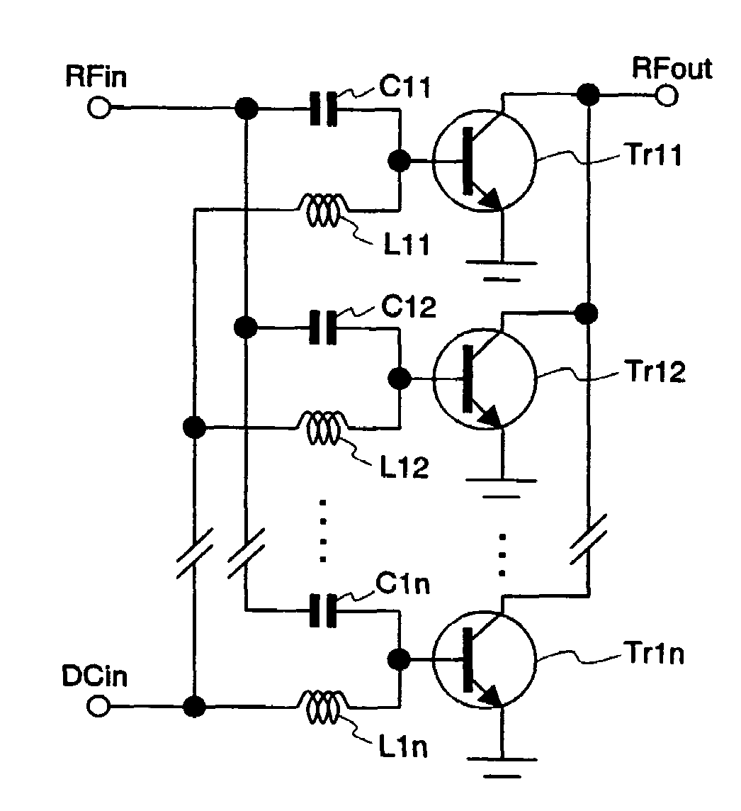
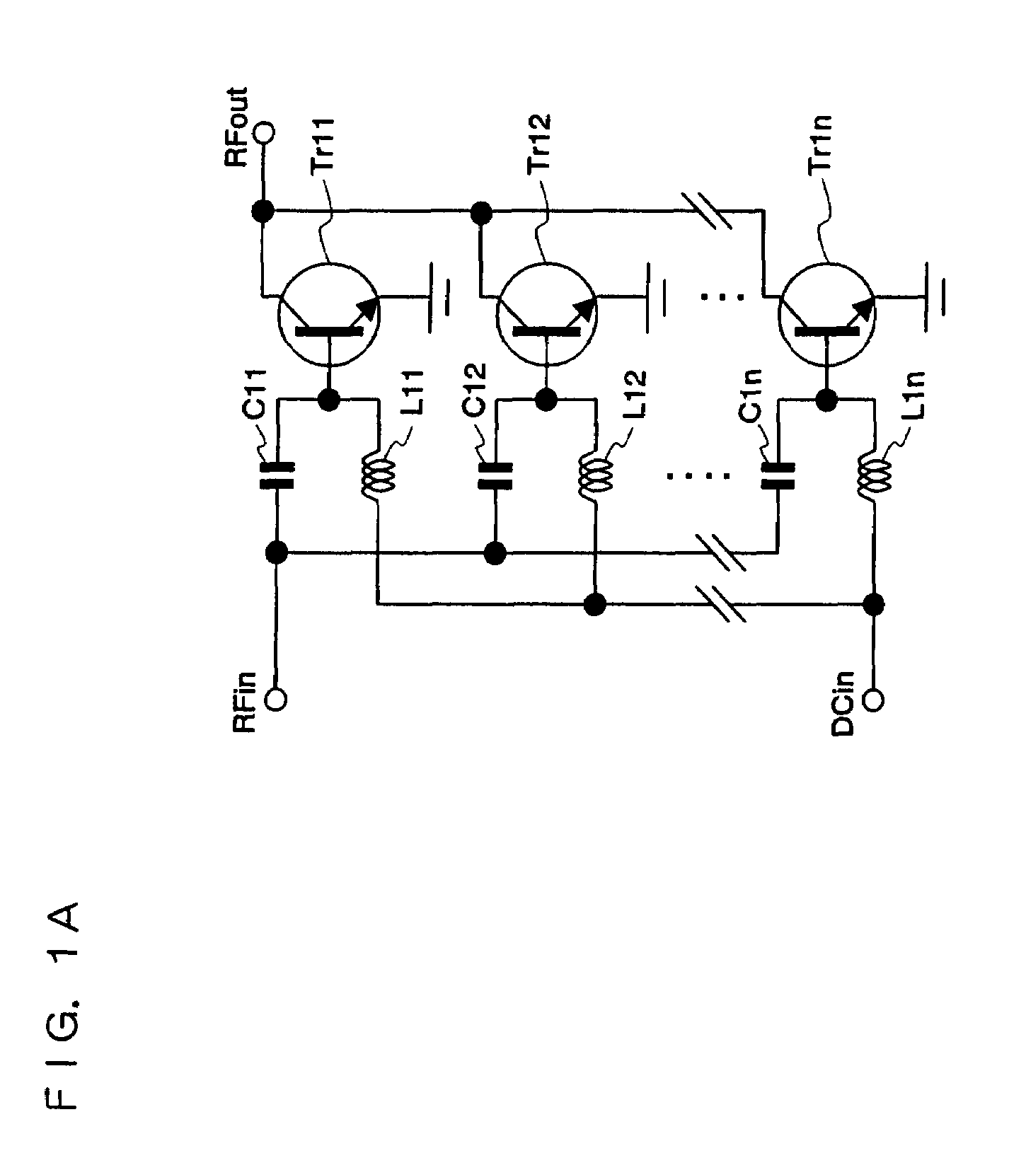
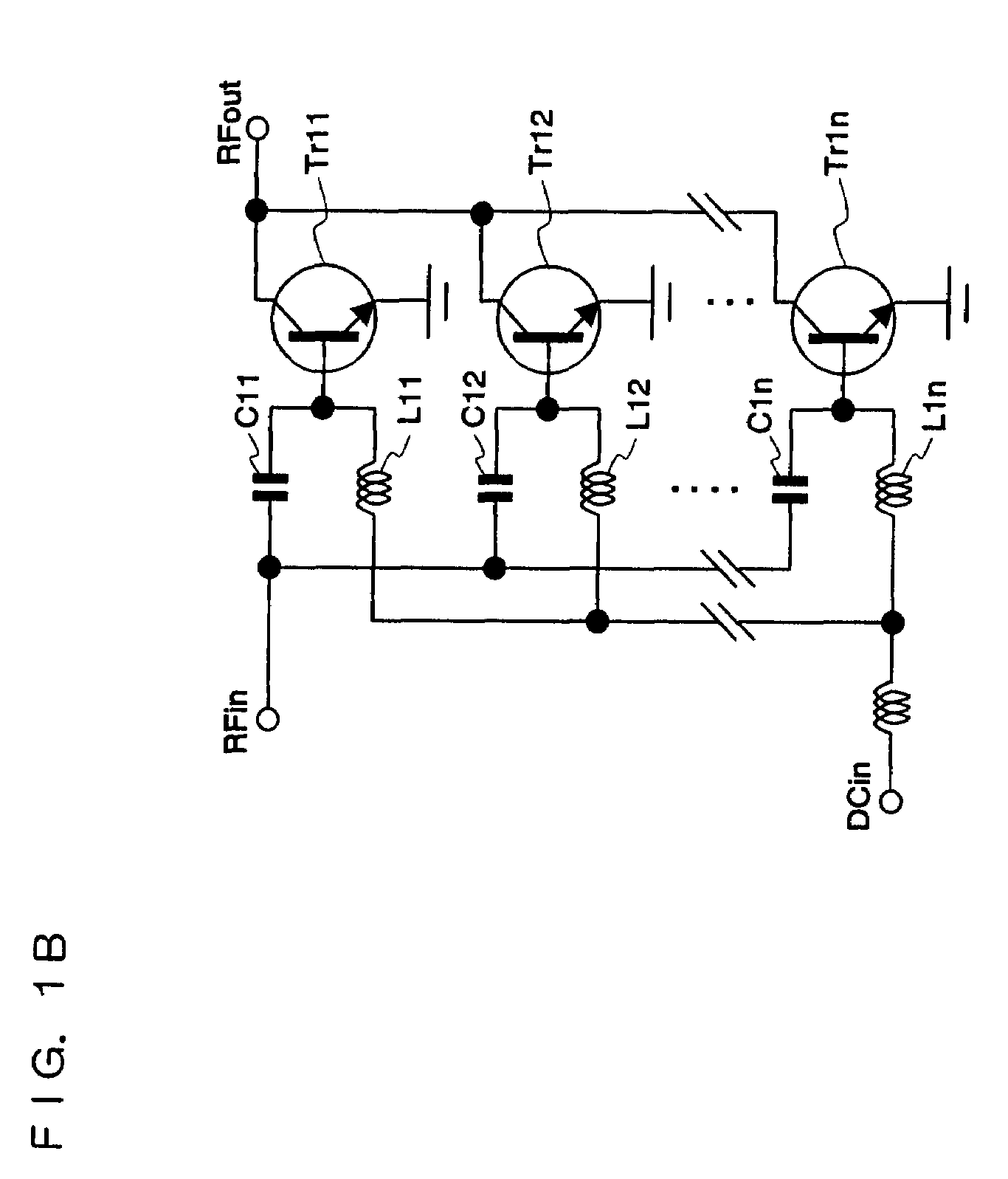
[0035]FIG. 1A is a circuit diagram of a transistor integrated circuit apparatus according to a first embodiment of the present invention. The transistor integrated circuit apparatus shown in FIG. 1A includes n number of transistors Tr11 through Tr1n, n number of capacitors C11 through C1n, n number of inductors L11 through L1n, a DC power supply input terminal DCin, an RF signal input terminal RFin, and an RF signal output terminal RFout. The transistor integrated circuit apparatus shown in FIG. 1A is entirely formed on one semiconductor substrate.

[0036]A base electrode of the transistor Tr11 is connected to one end of the capacitor C11 and one end of the inductor L11. The other end of the capacitor C11 is connected to the RF signal input terminal RFin. The other end of the inductor L11 is connected to the DC power supply input terminal DCin. A collector electrode of the transistor Tr11 is connected to the RF signal output terminal RFout, and an emitter electrode of the transistor T...

second embodiment

[0048]Next, a transistor integrated circuit apparatus according to a second embodiment of the present invention will be described. The transistor integrated circuit apparatus according to the second embodiment is different from the transistor integrated circuit apparatus according to the first embodiment in using a metal thin film as a material of the inductors. By using a metal for the inductors, the inductor obtains a resistance component. FIG. 3 shows an equivalent circuit of the transistor integrated circuit apparatus according to the second embodiment.

[0049]The transistor integrated circuit apparatus shown in FIG. 3 includes n number of transistors Tr31 through Tr3n, n number of capacitors C31 through C3n, n number of inductors L31 through L3n, and n number of bias resistors R31 through R3n. The bias resistors R31 through R3n are resistance components of the inductors L31 through L3n. In the following description, the transistor Tr31, the capacitor C31, the inductor L31 and the...


PUM


Abstract

A transistor integrated circuit apparatus generating less noise, having superb RF characteristics, and preventing thermal runaway of transistors is provided. Owing to capacitors C11 through C1n having one end commonly connected to an RF signal input terminal RFin and the other end connected to a base electrode of a corresponding transistor, and inductors L11 through L1n having one end commonly connected to a DC power supply input terminal DCin and the other end connected to a base electrode of a corresponding transistor, RF noise generated in a DC power supply circuit is reduced. This can reduce the RF noise output from the transistors Tr11 through Tr1n. The inductors L11 through L1n prevent an RF signal input from the RF input terminal RFin from flowing toward the DC power supply circuit. This can prevent the RF signal from being lost by the flow thereof toward the DC power supply circuit.

Description

BACKGROUND OF THE INVENTION[0001]1. Field of the Invention[0002]The present invention relates to a transistor integrated circuit apparatus, and more specifically to a transistor integrated circuit apparatus usable for, for example, a power transistor circuit for amplifying an RF signal.[0003]2. Description of the Background Art[0004]For a transistor circuit for amplifying an RF signal, a circuit including a plurality of transistors (for example, hetero-junction bipolar transistors) connected in parallel is conventionally used in order to guarantee good RF characteristics.[0005]For example, a circuit shown in FIG. 4 is conventionally used as a power transistor circuit. The power transistor shown in FIG. 4 includes n number of transistors Tr41 through Tr4n, a bias resistor R41, a capacitor C41, a DC power supply input terminal DCin, a RF signal input terminal RFin, and a RF signal output terminal RFout.[0006]In the power transistor circuit shown in FIG. 4, a DC voltage (bias voltage) ...

Claims


Application Information

Patent Timeline
Patent Type & Authority Patents(United States)
IPC IPC(8): H03F3/191
CPCH03F3/602H03F3/189
Inventor TATEOKA, KAZUKITARA, KATSUSHIMOTOYOSHI, KANAME
Owner COLLABO INNOVATIONS INC
Why Eureka
Try Eureka