Tunable photonic band gap structures for microwave signals

a photonic band gap and microwave signal technology, applied in the field of microwave components, can solve the problems of not being able to “switch off” and needing dielectric substrate drilling to create perforations, and achieve the effects of enhancing the lattice pattern, and reducing the number of holes

Inactive Publication Date: 2007-10-02
WU JAY HSING +3
View PDF4 Cites 15 Cited by
  • Summary
  • Abstract
  • Description
  • Claims
  • Application Information

AI Technical Summary

Benefits of technology

[0020]One objective of this invention is to provide a planar PBG structure with an enhanced lattice pattern to allow switching or tuning of its bandstop characteristics. The enhanced lattice pattern consists of several unit cells inside of a ground plane. Each unit cell is a perforation etched from the ground plane with a smaller conducting island deposited within the perforation. As a result, the conducting island is surrounded with a ring of gap where no ground metal is presented. A controllable thin film layer with variable conductivity is then deposited inside of the ring of gap and overlapping a portion of the ground plane and a portion of the conducting island so changing the conductivity of the controllable thin film layer can control the behavior of the bandstop. The conducting island inside of the perforation is electrically connected to the ground plane when the conductivity of the controllable thin film layer is high. Thus, the bandstop characteristics are eliminated since the ground plane is effectively electrically continuous (Refers to “bandstop-off” state shown in FIG. 2). On the other hand, the conducting island inside of the perforation is electrically isolated from the ground plane when the conductivity of the controllable thin film layer is low. The bandstop characteristics are therefore presented since the ground plane is not electrically continuous (Refers to “bandstop-on” state shown in FIG. 2). The controllable thin film could be a photoconductive material or a temperature sensitive material so that the conductivity can be changed by illumination or temperature variation. Furthermore, by adding the conducting island inside of the perforation, it becomes possible to switch on and off the bandstop characteristics very efficiently (ie, less optical power is required if a photoconductive material is used).
[0021]Another objective of the present invention is to provide a method to switch a PBG structure with enhanced lattice pattern. The method involves switching of freestanding thin films such as MEMS structures where four MEMS actuators are deposited at the corners of the conducting island. By controlling the mechanical switch of the MEMS actuators electrically, the bandstop characteristics can be switched.

Problems solved by technology

However, the drawback of the dielectric-based PBG structures is that drilling of the dielectric substrate is required to create the perforations.
Hence, in addition to the high light intensity requirement, it may not be possible to “switch off” the bandstop effect of the PBG structure 27.

Method used


Image

  • Tunable photonic band gap structures for microwave signals
  • Tunable photonic band gap structures for microwave signals
  • Tunable photonic band gap structures for microwave signals

Examples


Embodiment Construction

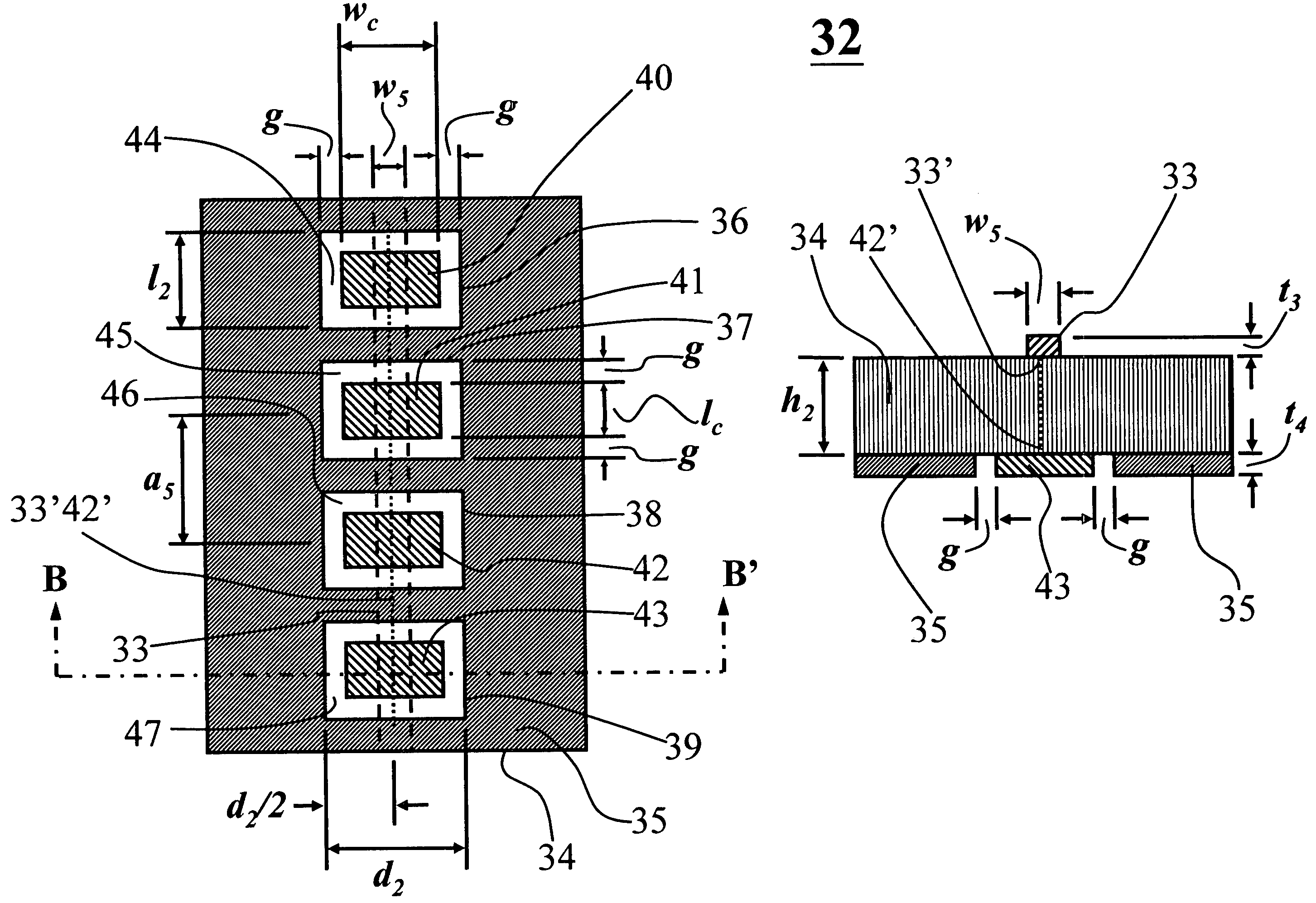
[0033]One objective of this invention is to achieve the switching or tuning of PBG bandstop characteristics so a distinct bandstop is seen (“bandstop-on” state) and such bandstop becomes bandpass when the PBG is switched to a “bandstop-off” state. FIGS. 6(a) and 6(b) show a top view and a cross-sectional view along B-B′ of a PBG structure 32 according to one embodiment of this invention. This PBG structure 32 consists of a microstrip line 33 with a width w5 and a thickness t3 deposited on the front surface of a dielectric substrate 34 of a thickness h2. A ground plane 35 with a thickness of t4 is deposited on the back surface of the dielectric substrate 34. The width w5 of the microstrip line 33 is selected according to the dielectric constant, thickness h2 of the electric substrate 34, and the impedance of the microstrip line required. Inside of the ground plane 35, four rectangular perforations 36, 37, 38, 39 with a length of l2 and a width of d2 are etched to form a one-dimension...


PUM


Abstract

Photonic Band Gap (PBG) structures are utilized in microwave components as filters to suppress unwanted signals because they have the ability to produce a bandstop effect at certain frequency range depending on the structural dimensions. The unique property of PBG structures is due to the periodic change of the dielectric permittivity so interferences are created with the traveling electromagnetic waves. Such periodic arrangement could exist either inside of the dielectric substrate or in the ground plane of a microstrip transmission line structure. This invention provides tunable or switchable planar PBG structures, which contains lattice pattern of periodic perforations inside of the ground plane. The tuning or switching of the bandstop characteristics is achieved by depositing a conducting island surrounded by a layer of controllable thin film with variable conductivities. The controllable thin film layer could be photoconductive or temperature sensitive that allows change in its conductivity to occur by means of light illumination or temperature variation. Instead of depositing the controllable thin film with variable conductivity, freestanding thin film such as MEMS structures can also be utilized as the medium between the conducting islands and the ground plane. According to this invention, bandstop characteristics of the planar PBG structure are switched off when the controllable thin film is conductive or the freestanding thin film is in contact with the conducting islands and the ground plane. Meanwhile the bandstop characteristics are switched on when the controllable thin film is resistive or the freestanding thin film is not in contact with the conducting islands. At the end, switching uniplanar-compact PBG (UC-PBG) structures with photoconductive or temperature sensitive material, which is deposited inside of the gaps located in the ground plane, is also described.

Description

BACKGROUND OF THE INVENTION[0001]1. Field of Invention[0002]This invention relates to a microwave component with a periodic lattice structure to achieve filtering and switching of microwave signals.[0003]2. Brief Description of the Prior Arts[0004]The term “Photonic Band Gap” (PBG) was initially used in optical regime where a strong reflection in a certain range of frequency is observed. Such reflection is caused by periodic changes of dielectric layers with different indices of refraction. Since the propagation of light is prohibited in such a range of frequency, it is referred to as the “band-gap” [E. Yablonovitch, Phys. Rev. Lett., 58, pp. 2059-2062, 1987]. This remarkable property inspires many researchers to put great efforts into the development of PBG structures in microwave and millimeter-wave components [Yongxi Qian and T. Itoh, 1999 IEEE MTT-S International, Microwave Symposium Digest, Vol. 4, pp. 13-19, June 1999]. Interests have been paid to microwave PBG structures beca...

Claims


Application Information

Patent Timeline
Patent Type & Authority Patents(United States)
IPC IPC(8): H01Q15/02H01P1/20H01P1/203
CPCH01P1/2039H01P1/2005
Inventor WU, JAY HSINGQIU, CHUNONGQIU, CINDY XINGSHIH, ISHIANG
Owner WU JAY HSING
Why Eureka
Try Eureka