Method and device for driving liquid crystal display

a liquid crystal display and display technology, applied in the field of liquid crystal display, can solve the problems of delay phenomenon, liquid crystal molecules, and require a period of time to develop targeted orientations, etc., and achieve the effect of fast optical response time, superior quality and fast changing

Inactive Publication Date: 2007-10-02
VASTVIEW TECH
View PDF3 Cites 10 Cited by
  • Summary
  • Abstract
  • Description
  • Claims
  • Application Information

AI Technical Summary

Benefits of technology

[0011]The present invention provides a method and device for overdriving a LCD display to effectively achieve faster optical response time so that fast changing; dynamic images can be displayed with superior quality.

Problems solved by technology

The LCD display, however, does have its own limitations.
The liquid crystal molecules, however, require a period of time to develop the targeted orientations.
The change of brightness of pixels therefore lags behind the change of voltages, causing a so-called delay phenomenon.
This delay phenomenon seriously affects the display quality of fast changing, dynamic images on a LCD display.
This is the major limitation of the overdrive method according to a prior art.

Method used


Image

  • Method and device for driving liquid crystal display
  • Method and device for driving liquid crystal display
  • Method and device for driving liquid crystal display

Examples


first embodiment

of the Present Invention

[0032]The first embodiment of the present invention is described in the following along with FIGS. 4(a) and 4(b) and FIGS. 5(a) to 5(e).

[0033]FIGS. 4(a) and 4(b) are schematic diagrams showing the overdrive device and an inner structure of a pixel at the intersection of a plurality of gate lines and data lines according to the first embodiment of the present invention.

Driving Device of the First Embodiment of the Present Invention

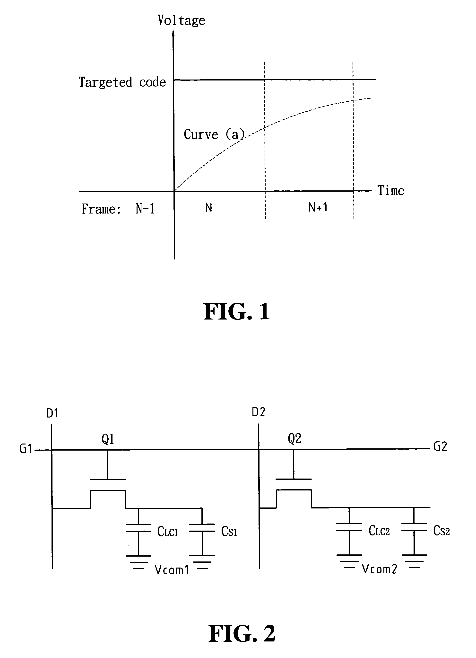
[0034]As shown in FIG. 4(b), the pixel structure of the overdrive device according to the present invention comprises a firs gate line G1, a second gate line G1′, a first data line D1, a second data line D1′, a first capacitor Cs connected to the ground as a storage capacitor, a second capacitor CLC also connected to the ground representing the equivalent capacitance of liquid crystal, an output line (not shown in FIG. 4(b)) for delivering the output overdrive voltage (VLC) to the a corresponding pixel on the LCD display, a first tra...

second embodiment

of the Present Invention

[0042]The second embodiment of the present invention is described in the following along with FIGS. 6(a) and 6(b) and FIGS. 7(a) to 7(g).

[0043]FIGS. 6(a) and 6(b) are schematic diagrams showing the overdrive device and an inner structure of a pixel at the intersection of a plurality of gate lines and data lines according to the second embodiment of the present invention.

Driving Device of the Second Embodiment of the Present Invention

[0044]As shown in FIG. 6(b), the pixel structure of the overdrive device according to the present invention comprises a firs gate line G1, a second gate line G1′, a first data line D1, a second data line D1′, a first capacitor Cs connected to the ground as a storage capacitor, a second capacitor CLC also connected to the ground representing the equivalent capacitance of liquid crystal, an output line (not shown in FIG. 6(b)) for delivering the output overdrive voltage (VLC) to a corresponding pixel on the LCD display, a first tran...

third embodiment

of the Present Invention

[0053]The third embodiment of the present invention is described in the following along with FIGS. 8(a) and 8(b) and FIGS. 9(a) to 9(d).

[0054]FIGS. 8(a) and 8(b) are schematic diagrams showing the overdrive device and an inner structure of a pixel at the intersection of a plurality of gate lines and data lines according to the third embodiment of the present invention.

Driving Device of the Third Embodiment of the Present Invention

[0055]As shown in FIG. 8(b), the pixel structure of the overdrive device according to the present invention comprises a firs gate line G1, a first data line D1, a first capacitor Cs connected to the ground as a storage capacitor, a second capacitor CLC also connected to the ground representing the equivalent capacitance of liquid crystal, an output line (not shown in FIG. 8(b)) for delivering the output overdrive voltage (VLC) to a corresponding pixel on the LCD display, a first transistor Q1 having its gate connected to the first ga...


PUM

PropertyMeasurementUnit
voltageaaaaaaaaaa
frame timeaaaaaaaaaa

Abstract

A method and device for overdriving a liquid crystal display is provided, which overcomes the limitations and disadvantages of prior arts. The invention can reduce the optical response time of liquid crystal to the driving voltage so that dynamic images can be displayed with superior quality. To achieve the objective of accelerating liquid crystal optical response, the basic pixel structure of the overdrive device provided by the invention contains a first gate line, a second gate line, a first data line, a second data line, a first capacitor, a second capacitor, an output line, a first transistor, and a second transistor. The first transistor has its gate connected to the first gate line, its source connected to the first data line, and its drain connected to the output line, the first capacitor, and the second transistor's drain. The second transistor has its gate connected to the second gate line, its source connected to the second data line, and its drain connected to the output line, the second capacitor, and the first transistor's drain. The first and second capacitors are also connected to the ground. The output line delivers the driving voltage to the corresponding pixel of the LCD display. The first and second gate lines are connected to a gate driver. The first and second data lines are connected to a data driver. The invention also provides a method for overdriving a liquid crystal display.

Description

BACKGROUND OF THE INVENTION[0001]1. Field of the Invention[0002]The present invention generally relates to the liquid crystal display, and more specifically to a device and method for driving the liquid crystal display.[0003]2. The Prior Arts[0004]A liquid crystal display (LCD), due to its small form factor, low power consumption, and low heat dissipation, has been widely utilized on various electronic devices. Especially, as the LCD technology has advanced to surpass the limitations and disadvantages of conventional or other existing display technologies such as cathode ray tube (CRT) and light emitting diode (LED), the LCD has been considered to have great importance and potential for the future development of computers, mobile handsets, and other consumer electronic devices.[0005]Generally, an LCD is made by two glass substrates with specially processed surfaces and liquid crystal molecules interposed therebetween. When applying different voltages on the electrodes of the glass s...

Claims


Application Information

Patent Timeline
Patent Type & Authority Patents(United States)
IPC IPC(8): G09G5/10G02F1/133G09G3/36
CPCG09G3/3659G09G2300/0809G09G2340/16G09G2320/0252G09G2320/0261G09G2310/0205
Inventor SHEN, YUH-RENCHEN, CHENG-JUNG
Owner VASTVIEW TECH
Why Eureka
Try Eureka