Semiconductor device cooling apparatus

a cooling apparatus and semiconductor technology, applied in the direction of cooling/ventilation/heating modification, semiconductor device details, semiconductor/solid-state device details, etc., can solve the problems of low cooling capability, high manufacturing cost, complex structure of semiconductor devices, etc., and achieve excellent cooling performance, low cost, and easy and accurate formation

Inactive Publication Date: 2007-10-09
FUJITSU LTD
View PDF13 Cites 15 Cited by
  • Summary
  • Abstract
  • Description
  • Claims
  • Application Information

AI Technical Summary

Benefits of technology

[0014]The present invention has been made in view of the above circumstances and provides a semiconductor device cooling apparatus that can uniformly cool a semiconductor device excellently by a simple structure.
[0016]In the semiconductor device cooling apparatus of the present invention, since a thin laminar flow of coolant (water) is formed along the inner surface of the heat transmission plate by forming the gap-shaped flow path having the small height, a high heat absorption capability can be obtained by a relatively simple structure. Further, the gap-shaped flow path is a flow path that allows a coolant supplied to the central portion of the inner surface of the heat transmission plate to radially flow from central portion of the heat transmission plate toward the peripheral edge portion thereof so that the semiconductor device can be uniformly cooled.
[0018]The gap-shaped flow path can be simply, easily and accurately formed at a low cost by the combination of the gap forming plate and the elastic member.
[0019]As described above, according to the present invention, a semiconductor device can be uniformly and excellently cooled by the relatively simple structure.

Problems solved by technology

The cooling plate 20 having the groove type flow paths 24a and 24b is disadvantageous in that the structure of it is complex and a manufacturing cost is expensive, although a high cooling performance can be easily obtained when the semiconductor device 10 is cooled thereby.
While the cooling plate having the tube type flow path as shown in FIGS. 2(A) and 2(B) can be made at a relatively low cost, the cooling plate is disadvantageous in that it has a low cooling capability and it is difficult to reduce its size.
However, since the coolant flows in the one direction, for example, from right to left, it has a temperature gradient between the right side and the left side thereof, from which a problem arises in that the coolant has a different heat absorption capability on the right side and the left side of a semiconductor device and it is difficult to uniformly cool the semiconductor device by the flow path structure.

Method used


Image

  • Semiconductor device cooling apparatus
  • Semiconductor device cooling apparatus
  • Semiconductor device cooling apparatus

Examples


Embodiment Construction

[0028]Embodiments of the present invention will be explained below.

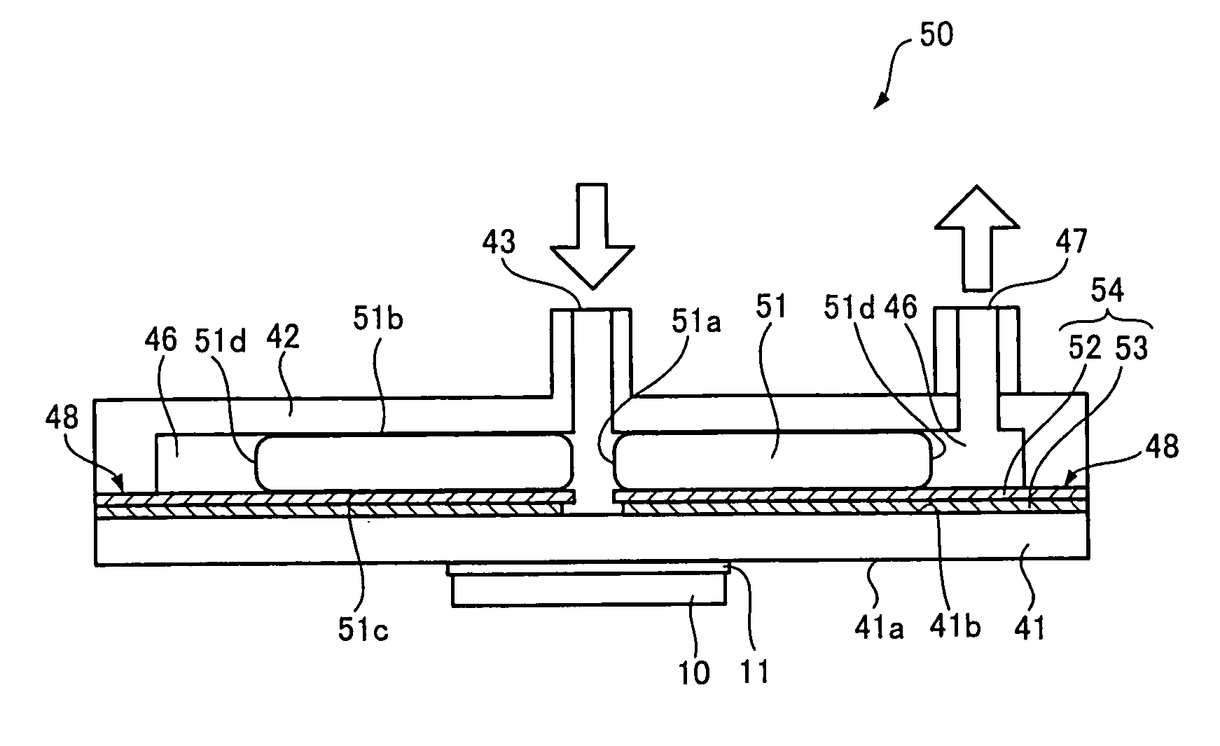
[0029]FIG. 3 is a longitudinal sectional view showing a cooling plate as a first embodiment of a semiconductor device cooling apparatus of the present invention, and FIG. 4 is a plan view of the cooling plate of the first embodiment. FIG. 3 is a sectional view of the cooling plate taken along the arrow-carrying line Y—Y of FIG. 4. Note that the sectional view of the cooling plate in FIG. 3 is larger than the plan view of it in FIG. 4 for the easy comprehension of it.

[0030]The cooling plate 40 shown in FIGS. 3 and 4 is provided with a heat transmission plate 41 having an outer surface 41a on which a semiconductor device 10 is closely fixed with a thermal joint member 11 such as a solder, an adhesive, a thermal grease, a thermal sheet, and the like.

[0031]Further, a housing 42 has an annular projection 44 having a hole 44a defined at a center, and the hole 44a is connected to a supply port 43. The annular projection 44 ...


PUM


Abstract

In a semiconductor device cooling apparatus which cools a semiconductor device uniformly with a simple structure, a coolant is supplied from a supply port to the center of a heat transmission plate on which a semiconductor device is disposed in intimate contact therewith, is radially flown toward the peripheral edge portion of the heat transmission plate through a gap-shaped flow path which is formed by a gap forming plate composed of two thin plate members of a gap interval plate acting as a spacer and a gap top plate disposed on the gap interval plate and has a small height, is collected by a collection groove formed around the peripheral edge portion, and is discharged from a discharge port.

Description

BACKGROUND OF THE INVENTION[0001]1. Field of the Invention[0002]The present invention relates to a semiconductor device cooling apparatus used to cool a semiconductor device with a liquid.[0003]2. Description of the Related Art[0004]Heretofore, various types of structural parts for cooling semiconductor devices are proposed, and, in particular, various groove type and tube type coolant flow path structures are conventionally used often to a semiconductor device cooling apparatus called a cooling plate that is used to cool a semiconductor device by a fluid.[0005]FIGS. 1(A) and 1(B) are views showing a schematic structure of a cooling plate having groove type flow paths, wherein FIG. 1(A) is a sectional plan view of the cooling plate taken along the arrow-carrying line X—X of the cooling plate shown in FIG. 1(B), and FIG. 1(B) is a side view of the cooling plate.[0006]The cooling plate 20 includes a heat transmission plate 21, a semiconductor device 10 is joined to an outer surface 21...

Claims


Application Information

Patent Timeline
Patent Type & Authority Patents(United States)
IPC IPC(8): H05K7/20
CPCH01L23/473H01L2924/0002H01L2924/00
Inventor FUJISAKI, AKIHIKO
Owner FUJITSU LTD
Why Eureka
Try Eureka