Semiconductor memory device

a memory device and semiconductor technology, applied in the field of semiconductor memory devices, can solve the problems of unnecessary current consumption in idle state or active state of bank, and achieve the effect of reducing an unnecessary current consumption

Active Publication Date: 2007-10-09
SK HYNIX INC
View PDF12 Cites 39 Cited by
  • Summary
  • Abstract
  • Description
  • Claims
  • Application Information

AI Technical Summary

Benefits of technology

[0052]It is, therefore, an object of the present invention to provide a semiconductor memory device for reducing an unnecessary current consumption occurred in an idle state or an active state.
[0053]In accordance with an aspect of the present invention, there is provided a semiconductor memory device for reducing an unnecessary current consumption, including a driving clock supply unit for supplying a driving clock during a read or a write operation of each bank; a delay unit for generating a read address or a write address in synchronization with the driving clock by delaying an address by a predetermined time based on one of an additive latency, a CAS latency and a combination thereof; and an output unit for latching the read address or the write address to output the latched signal as an internal column address.
[0054]In accordance with another aspect of the present invention, there is provided a semiconductor memory device for reducing an unnecessary current consumption, including a first driving clock supply unit for supplying a first driving clock during a read or a write operation of each bank; a second driving clock supply unit for supplying a second driving clock during the write operation of each bank; a read address generating unit for generating an AL address in synchronization with the first driving clock by delaying an address inputted in response to a CAS signal by an additive latency to thereby output a read address according to a read CAS signal; a write address generating unit for generating a CL address in synchronization with the second driving clock by delaying the AL address by a CAS latency to thereby output a write address according to a write CAS signal; and an address output unit for latching the read address or the write address to output the latched signal as an internal column address.

Problems solved by technology

In the conventional semiconductor memory device, because of generating the internal column address, a problem that an unnecessary current consumption in an idle state or an active state of bank is occurred has arisen.

Method used


Image

  • Semiconductor memory device
  • Semiconductor memory device
  • Semiconductor memory device

Examples


Embodiment Construction

[0069]Hereinafter, a semiconductor memory device in accordance with the present invention will be described in detail referring to the accompanying drawings.

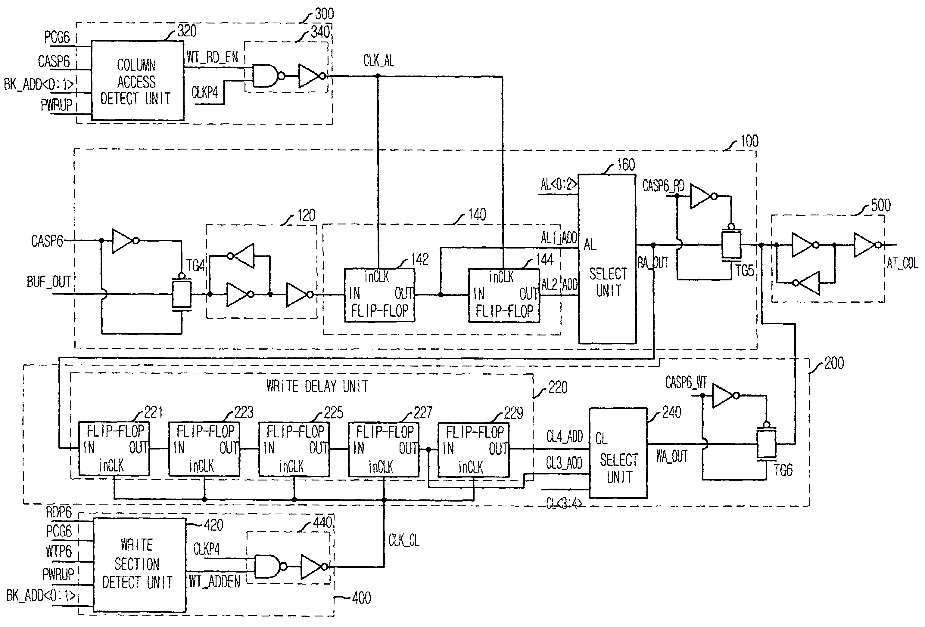
[0070]FIG. 6 is a block diagram showing a column address shift unit in a semiconductor memory device in accordance with an embodiment of the present invention.

[0071]As shown, the semiconductor memory device of the present invention includes a read address generating unit 100, a write address generating unit 200, a first driving clock supply unit 300, a second driving clock supply unit 400 and an address output unit 500.

[0072]The first driving clock supply unit 300 supplies a first driving clock CLK_AL for the read address generating unit 100 during a read or a write operation in a corresponding bank. The second driving clock supply unit 400 supplies a second driving clock CLK_CL for the write address generating unit 200 during the write operation in the corresponding bank. The read address generating unit 100 generates an AL add...


PUM


Abstract

Disclosed herein is a semiconductor memory device for reducing an unnecessary current consumption occurred in an idle state or an active state. The semiconductor memory device includes a driving clock supply unit for supplying a driving clock during a read or a write operation of each bank; a delay unit for generating a read address or a write address in synchronization with the driving clock by delaying an address by a predetermined time based on one of an additive latency, a CAS latency and a combination thereof; and an output unit for latching the read address or the write address to output the latched signal as an internal column address.

Description

FIELD OF THE INVENTION[0001]The present invention relates to a semiconductor memory device; and, more particularly, to a semiconductor memory device for reducing an unnecessary current consumption occurred in an idle state or an active state.DESCRIPTION OF RELATED ART[0002]Generally, to access a predetermined cell in a semiconductor memory device, an operation to select a wordline and a bitline connected to the specific cell is required. Also, to select the wordline and the bitline, a command and an address relating to the predetermined cell are inputted. The semiconductor memory device performs an operation corresponding to the command and the address of the predetermined cell for a predetermined time.[0003]For example, it is assumed that a row active command and a row address for activating the wordline are loaded to the semiconductor memory device. After a row address strobe (Hereinafter, referred to a RAS) to column address strobe (Hereinafter, referred to a CAS) delay time tRCD...

Claims


Application Information

Patent Timeline
Patent Type & Authority Patents(United States)
IPC IPC(8): G11C8/00
CPCG11C7/1066G11C11/4076G11C7/22G11C7/1072G06F3/04886G06F3/041H04M1/724
Inventor LEE, CHANG-HYUK
Owner SK HYNIX INC
Why Eureka
Try Eureka