Flat panel display with improved white balance

Active Publication Date: 2007-10-23
SAMSUNG DISPLAY CO LTD
View PDF4 Cites 9 Cited by
  • Summary
  • Abstract
  • Description
  • Claims
  • Application Information

AI Technical Summary

Benefits of technology

[0013]It is an aspect of the present invention to provide a flat panel display

Problems solved by technology

However, in the conventional method for embodying the white balance described above, since the light emitting area of the unit pixel having low luminous efficiency among the R, G and B unit pixels is enlarged, or the size of the transisto

Method used


Image

  • Flat panel display with improved white balance
  • Flat panel display with improved white balance
  • Flat panel display with improved white balance

Examples


first embodiment

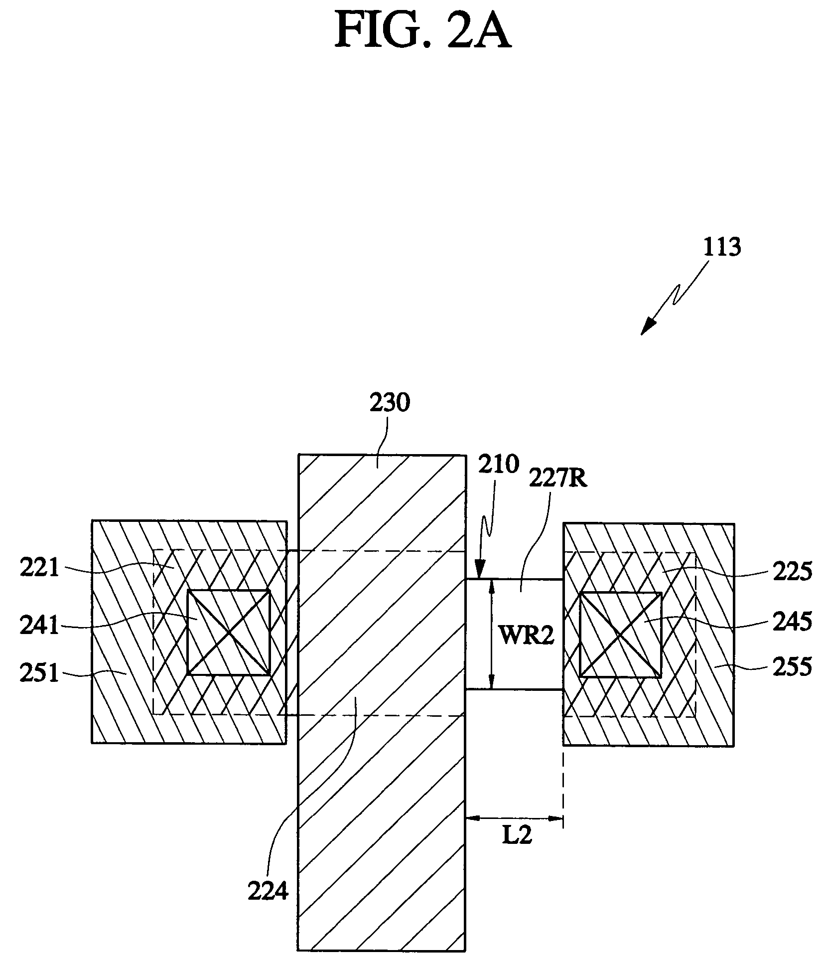
[0038]FIGS. 2A, 2B and 2C show plane structures of organic light emitting diodes in accordance with the present invention, with each figure showing driving transistors of R, G and B unit pixels.

[0039]Referring to FIGS. 2A, 2B and 2C, the driving transistors 113, 123 and 133 of the R, G and B unit pixels in accordance with the first embodiment of the present invention each include a semiconductor layer 210, a gate 230 and source / drain electrodes 251 and 255. The semiconductor layer 210 includes a channel layer 224 formed on a part corresponding to the gate 230 and high concentration source / drain regions 221 and 225 formed at both sides of the channel layer 224. Here, the source / drain regions 221 and 225 are electrically connected to the source / drain electrodes 251 and 255 through contacts 241 and 245, respectively.

[0040]As for the driving transistors 113, 123 and 133 of the R, G and B unit pixels, the semiconductor layers 210 of each further include offset regions 227R, 227G and 227B...

second embodiment

[0041]FIGS. 3A, 3B and 3C are views showing plane structures of an organic light emitting diode in accordance with the present invention, with each figure showing driving transistors of the R, G and B unit pixels, respectively.

[0042]Referring to FIGS. 3A, 3B and 3c, driving transistors 113, 123 and 133 of the R, G and B unit pixels in accordance with the second embodiment of the present invention each include a semiconductor layer 310, a gate 330 and source / drain electrode 351 and 355. The semiconductor layer 310 includes a channel layer 324 formed on a part corresponding to the gate 330 and high concentration regions 321 and 325 formed at both sides of the channel layer 324. The source / drain regions 321 and 325 are electrically connected to the source / drain electrodes 351 and 355 through contacts 341 and 345, respectively.

[0043]As for driving transistors 113, 123 and 133 of each R, G and B unit pixel, the semiconductor layer 310 of each further include offset regions 327R, 327G and...

third embodiment

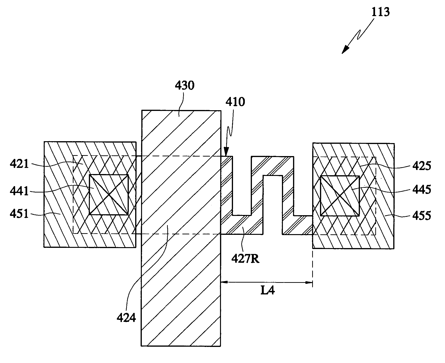
[0046]FIGS. 4A, 4B and 4C are views showing plane structures of an organic light emitting diode in accordance with the present invention, with each figure showing driving transistors of R, G and B unit pixels, respectively.

[0047]Referring to FIGS. 4A, 4B and 4C, the driving transistors 113, 123 and 133 of the R, G and B unit pixels in accordance with the third embodiment of the present invention each include a semiconductor layer 410, a gate 430 and source / drain electrodes 451 and 455. The semiconductor layer 410 includes a channel layer 424 formed on a part corresponding to the gate 430, and high concentration source / drain regions 421 and 425 formed at both sides of the channel layer 424. The source / drain regions 421 and 425 are electrically connected to the source / drain electrodes 451 and 455 through contacts 441 and 445, respectively.

[0048]As for driving transistors 113, 123 and 133 of each R, G and B unit pixel, the semiconductor layer 410 of each further include offset regions ...


PUM


Abstract

Disclosed is a flat panel display capable of enhancing a white balance by making a doping concentration or shape and size of drain offset regions of driving transistors different, in R, G and B unit pixels of each pixel. A flat panel display, comprises a plurality of pixels, where each of pixels including R, G and B unit pixels to embody red (R), green (G) and blue (B) colors, respectively. Each of the unit pixels includes a transistor with source/drain regions. Transistors of at least two unit pixels of the R, G and B unit pixels have drain regions of different geometric structures. In each unit pixel, a resistance value of the drain region of the transistor to drive a light-emitting device having the highest luminous efficiency among the transistors is higher than that of the drain region of a transistor to drive the light-emitting device having a relatively low luminous efficiency.

Description

CROSS-REFERENCE TO RELATED APPLICATION[0001]This application claims the benefit of Korean Patent Application No. 2003-24425 and 2003-24447, filed Apr. 17, 2003, the disclosure of which is incorporated herein by reference in its entirety.FIELD OF THE INVENTION[0002]The present invention is related to a full-color flat panel display and, more particularly, to a flat panel display capable of embodying a white balance by changing a doping concentration or shape and size of an offset in a drain region and then varying a resistance value of the drain region in each unit pixel.BACKGROUND OF THE INVENTION[0003]Generally, as shown in FIG. 1, an organic light emitting diode (OLED) being a flat panel display includes a number of pixels 100 which are arranged in the form of a matrix, each pixel 100 comprising three unit pixels, that is, a unit pixel 110R for embodying a red color (R), a unit pixel 120G for embodying a green color (G) and a unit pixel 130B for embodying a blue color (B).[0004]Th...

Claims


Application Information

Patent Timeline
IPC IPC(8): H01J1/62H01J63/04G09F9/30G09G3/20G09G3/32H01L21/77H01L27/12H01L27/32H01L29/786H05B33/00
CPCH01L27/12H01L29/78624H01L27/1214H01L27/3262H01L27/3211H01L27/1222H10K59/352H10K59/353H10K59/1213
Inventor KOO, JAE-BONPARK, SANG-ILLEE, UL-HOKIM, JIN-SOOJUNG, JIN-WOUNGLEE, CHANG-GYU
Owner SAMSUNG DISPLAY CO LTD
Why Eureka
Try Eureka