Configurable clock network for programmable logic device

a programmable logic and clock network technology, applied in the direction of generating/distributing signals, pulse techniques, instruments, etc., can solve the problems of high chip area cost, high power cost of implementation, and limited flexibility in assigning a particular clock source to a particular channel, so as to achieve the effect of not exceeding the area or power cos

Inactive Publication Date: 2007-10-23
TAHOE RES LTD
View PDF106 Cites 9 Cited by
  • Summary
  • Abstract
  • Description
  • Claims
  • Application Information

AI Technical Summary

Benefits of technology

[0008]The present invention allows the distribution of a plurality of clocks to serial data channels without excessive area or power cost by providing a segmented clock bus to which all of the available clocks may be connected. Different segments of the bus may be connectable to different clocks, or the entire bus may be connected to one clock.
[0009]Thus, if more than one clock is being provided, then as long as each serial data channel is located near a segment on which the particular clock that it requires is provided, all channels can receive the correct clocks. Because only one bus is used, it is not necessary to consume area or power with multiple buses, although some additional circuitry will be required to achieve the bus segmentation and to allow the various clocks to be selectively connected to the bus. Although the user may be constrained when programming the device to place all channels requiring a particular clock near one another—or, more particularly, near the segment of the bus carrying that particular clock—the user has much greater flexibility in deciding which channels will use which clocks than in an arrangement where groups of channels are dedicated to particular clocks. And although the user may have less flexibility than in an implementation where a separate bus if provided for each clock to allow any channel to access any bus, the present invention has much lower power and chip area costs than in such a multiple bus limitation.

Problems solved by technology

However, heretofore the flexibility to assign a particular clock source to a particular channel was limited.
The latter implementation requires a number of clock buses equal to the number of clock sources, as well as a plurality of—e.g., eight—multiplexers (each clock signal actually may be eight signals as described above) per channel per bus, imposing a high chip area cost.
This latter implementation also has a high power cost unless provision is made to power down unused buses, and in some user implementations there may not be any unused buses—if even one channel uses a particular clock source, then the entire bus for that clock source must be powered up.

Method used


Image

  • Configurable clock network for programmable logic device
  • Configurable clock network for programmable logic device
  • Configurable clock network for programmable logic device

Examples


embodiment 33

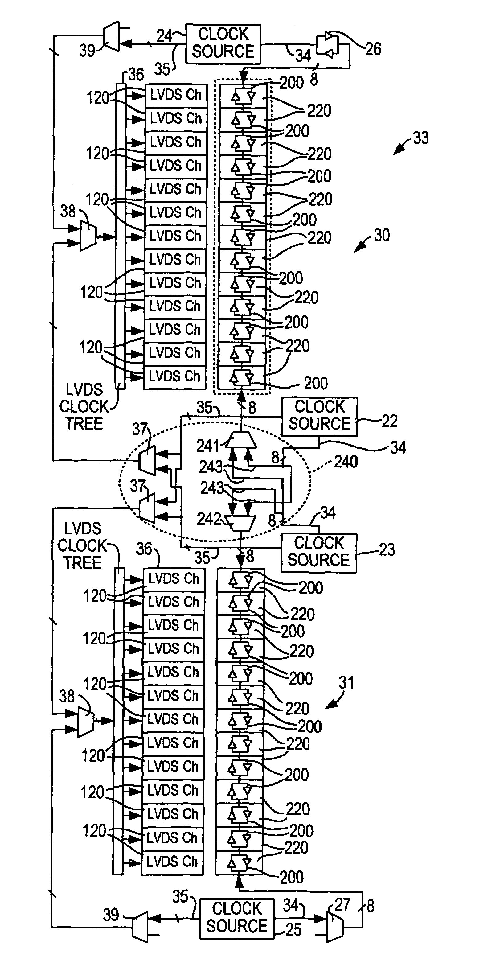
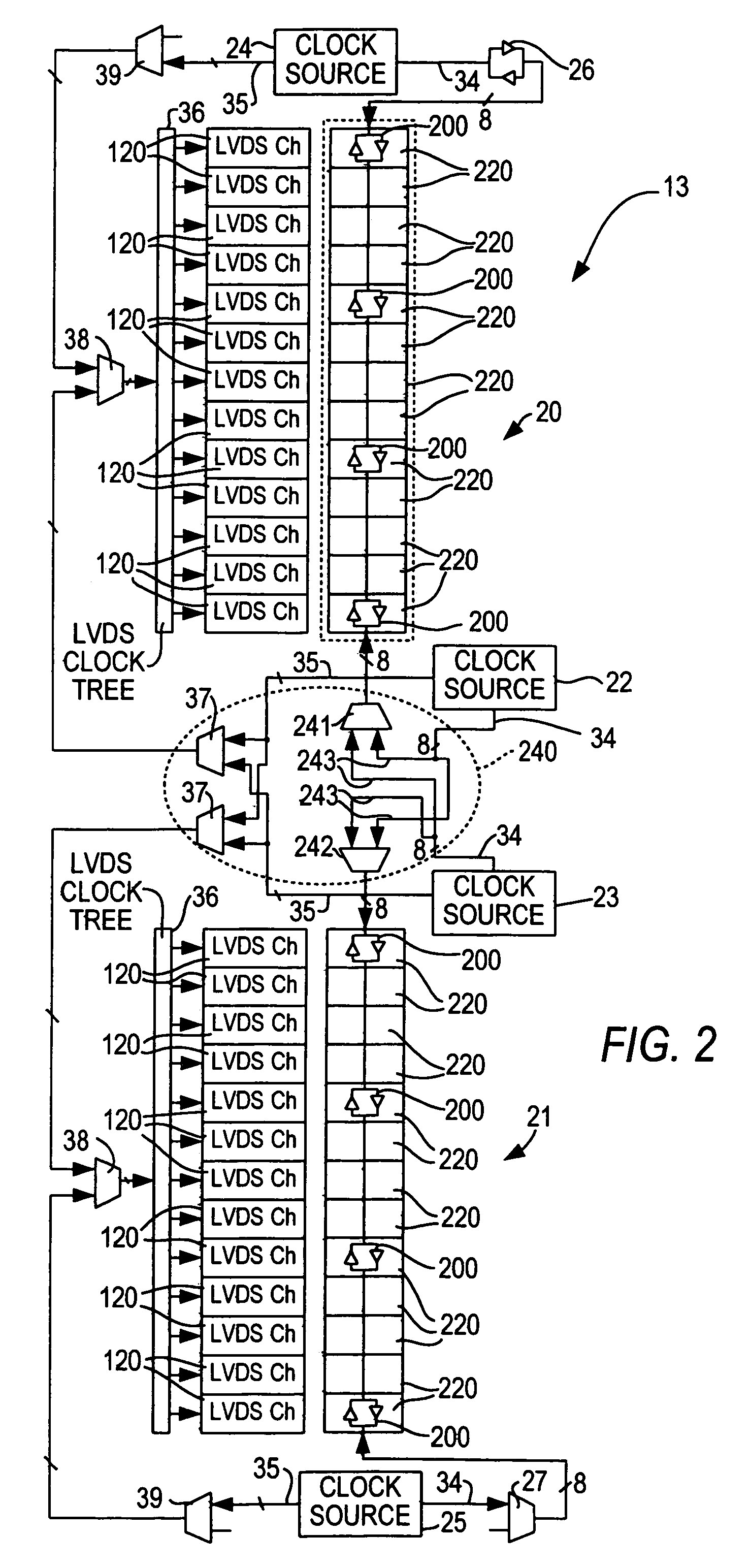
[0027]Because the tristatable buffers 200 are located at every fourth channel 220 in the embodiment shown in FIG. 2, if the user desires to segment either of clock distribution network portions 20, 21 into two clock buses, the user would be limited as to where those divisions could be made, and therefore as to how many of channels 220 could be assigned to each of those two clock buses. In the alternate embodiment 33 of FIG. 3, however, tristatable buffers 200 are located at each channel 220. Therefore, the user can segment each of clock network distribution portions 30, 31 at a point between any two channels, as may be desired.

[0028]It can be seen that in FIGS. 2 and 3 that in embodiments 13, 33, it may be possible in one configuration to have all channels 220 on a single clock bus connected to one of clock sources 22, 23. In a second configuration, it is possible to have all of clock distribution network portion 20, 30 be one clock bus connected to any one of clock sources 22, 23, ...

embodiment 43

[0035]As in the embodiments of FIGS. 2 and 3, above, in embodiment 43 of FIG. 4, a channel or group of channels could be skipped and the clock signal passed through to adjacent channels. However, in this embodiment, if any one of tristatable buffers 200 is tristated, then no channel beyond that point would receive clock signal. Thus, in this embodiment a tristatable buffer 200 would be tristated only when it is desired to skip all channels beyond that point. Preferably, in such a case, the circuitry (e.g., a passgate) discussed above would be used to force the unused clock conductors to a known state to prevent unnecessary power consumption.

[0036]Thus it can be seen that in accordance with the present invention, a single bus can be used to conduct multiple clock sources to different channels. Because each of these sources is actually, as discussed above, multiple (e.g., eight) phases of a single clock, the invention provides a significant savings in the number of bus conductors that...


PUM


Abstract

In a programmable logic device having high-speed serial interface channels, a clock distribution network for providing one or more high-speed clocks to dynamic phase alignment circuitry of those high-speed serial interfaces includes at least one bus that is segmentable (e.g. using tristatable buffers). This allows the bus to be divided into different portions that can be connected to different clock sources when the high-speed serial interfaces are running at different speeds. In one embodiment, the segmenting elements (e.g., the aforementioned buffers) are located between selected channels (e.g., every fourth channel), limiting the size of the different segments. In another embodiment, segmenting elements are located between each channel, allowing complete user freedom in selecting the sizes of the segments. Thus, instead of providing a bus for every clock source, multiple clocks can be made available to different channels by segmenting a single bus.

Description

CROSS REFERENCE TO RELATED APPLICATION[0001]This is a continuation of commonly-assigned U.S. patent application Ser. No. 10 / 830,562, filed Apr. 22, 2004, now U.S. Pat. No. 7,075,365.BACKGROUND OF THE INVENTION[0002]This invention relates to a configurable clock network for a programmable logic device. More particularly, this invention relates to a clock network that allows each of several clocks to be configurably routed to different portions of a programmable logic device.[0003]High-speed serial signaling is becoming an increasingly important form of signaling between electronic devices. For example, Low Voltage Differential Signaling (“LVDS”) has become a common form of signaling. Typically the data represent bytes of information that are being transmitted-one after another. The usual definition of a byte is eight bits, but as used herein “byte” can refer to any plural number of bits such as eight bits, nine bits, ten bits, eleven bits, or fewer or more than these numbers of bits....

Claims


Application Information

Patent Timeline
Patent Type & Authority Patents(United States)
IPC IPC(8): H01L25/00
CPCH03K19/017581G06F1/10
Inventor STARR, GREGORYWEI LAI, KANGCHANG, RICHARD Y
Owner TAHOE RES LTD
Why Eureka
Try Eureka