Transparent conductor

a conductor and transparent technology, applied in the direction of insulated conductors, cables, instruments, etc., can solve the problems of difficult to specify a touch position, difficult to fix, and damage to the surface of the transparent thin-film electrode layer of the inner transparent electrode disposed on the display side opposite the outer transparent electrode, so as to reduce the production of newton's rings, improve durability, and reduce the damage to the surface more reliably

Inactive Publication Date: 2007-10-30
TDK CORPARATION
View PDF4 Cites 2 Cited by
  • Summary
  • Abstract
  • Description
  • Claims
  • Application Information

AI Technical Summary

Benefits of technology

[0006]The present invention was conceived in view of the problem described above, and it is a principal object of the present invention to provide a transparent conductor that can prevent Newton's rings from being produced and can reduce the incidence of damage.
[0008]According to the above transparent conductor, the transparent conductive layer is formed so that a maximum peak height that shows a surface roughness of the surface is in a range of 0.35 μm to 0.43 μm, inclusive. With this construction, light is appropriately scattered, and therefore the production of Newton's rings can be reliably avoided. Also, unlike a conventional transparent conductor where the maximum peak height is large, by setting the maximum peak height in a range of 0.35 μm to 0.43 μm, inclusive, the heights of the peaks can be averaged, so that when an upper electrode and a lower electrode slide against each other, the pressure is distributed among the peaks and it is therefore possible to reliably reduce damage to the surfaces. Accordingly, with a touch panel in which the transparent conductor described above is incorporated, it is possible to reliably prevent the production of Newton's rings and to sufficiently improve durability.
[0010]According to the above transparent conductor, the transparent conductive layer is formed so that a maximum valley depth that shows a surface roughness of the surface is in a range of 1.03 μm to 2.37 μm, inclusive. With this construction, light is appropriately scattered, and therefore the production of Newton's rings can be reliably avoided. Also, unlike a conventional transparent conductor where the maximum valley depth is small, by setting the maximum valley depth in a range of 1.03 μm to 2.37 μm, inclusive, it is possible to reduce the number of peaks proportionate to the increase in the number of valleys, so that when an upper electrode and a lower electrode slide against each other, it is possible to reliably reduce damage to the surfaces. Accordingly, with a touch panel in which the transparent conductor described above is incorporated, it is possible to reliably prevent the production of Newton's rings and to sufficiently improve durability.
[0012]According to the above transparent conductor, the transparent conductive layer is formed so that a maximum peak height that shows a surface roughness of the surface is in a range of 0.35 μm to 0.43 μm, inclusive and a maximum valley depth that shows the surface roughness of the surface is in a range of 1.03 μm to 2.37 μm, inclusive. With the above construction, it is possible to average the heights of the peaks and to reduce the number of peaks proportionate to the increase in the number of valleys, and therefore the pressure can be distributed among the peaks when an upper electrode and a lower electrode slide against each other and the frequency of contact between the peaks and the surface of the lower electrode can be reduced. As a result, it is possible to reduce damage to the surfaces more reliably. Accordingly, with a touch panel in which the transparent conductor described above is incorporated, it is possible to reliably reduce the production of Newton's rings and to significantly improve durability.
[0013]Here, the transparent conductive layer may be constructed by compressing conductive fine particles. With this construction, it is possible to increase the points of contact between the conductive fine particles and to increase the contact area, thereby increasing the strength of the transparent conductive layer and improving the light transmittance of the transparent conductive layer. Also, unlike a conventional method of manufacturing that applies a coating composition including conductive fine particles and binder (resin) when forming the transparent conductive layer, it is possible to form the transparent conductive layer by applying a coating composition (dispersion liquid) that does not include resin and then compressing conductive fine particles, and therefore it is possible to reduce the probability of a fall in conductivity due to contact between the conductive fine particles being obstructed by the binder.

Problems solved by technology

However, even when the center line average roughness and maximum height are within the set ranges, for example, if the parts that protrude from the center line (average line) (hereinafter such parts are referred to as “peaks”) are high, when the transparent thin-film electrode layer is incorporated in a touch panel and touch operations are repeatedly performed, the surface of the transparent thin-film electrode layer of an inner transparent electrode disposed on the display side opposite the outer transparent electrode can be damaged by the peaks.
In this type of touch panel, when the surface of a transparent thin-film electrode layer is damaged, the resistance of the transparent thin-film electrode layer changes, resulting in a problem that it can be difficult to specify a touched position.

Method used


Image

  • Transparent conductor
  • Transparent conductor
  • Transparent conductor

Examples


Embodiment Construction

[0026]Preferred embodiments of a transparent conductor according to the present invention will now be described with reference to the attached drawings.

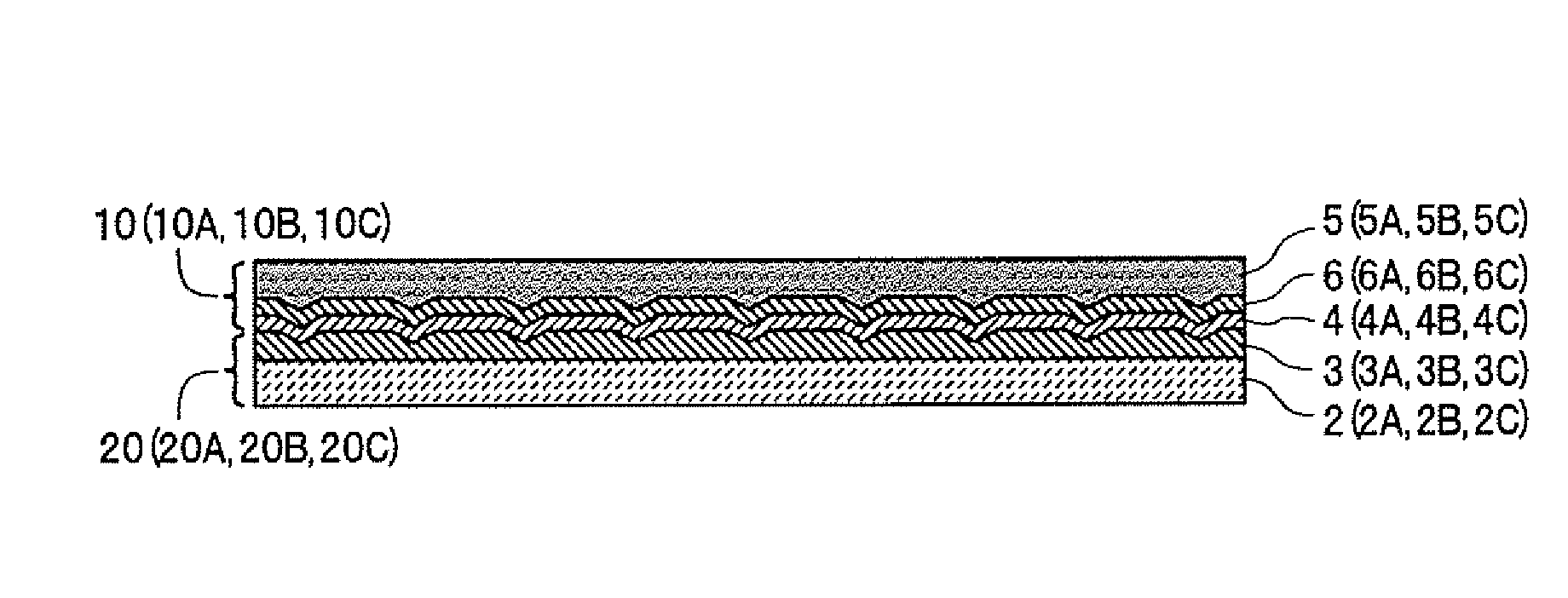
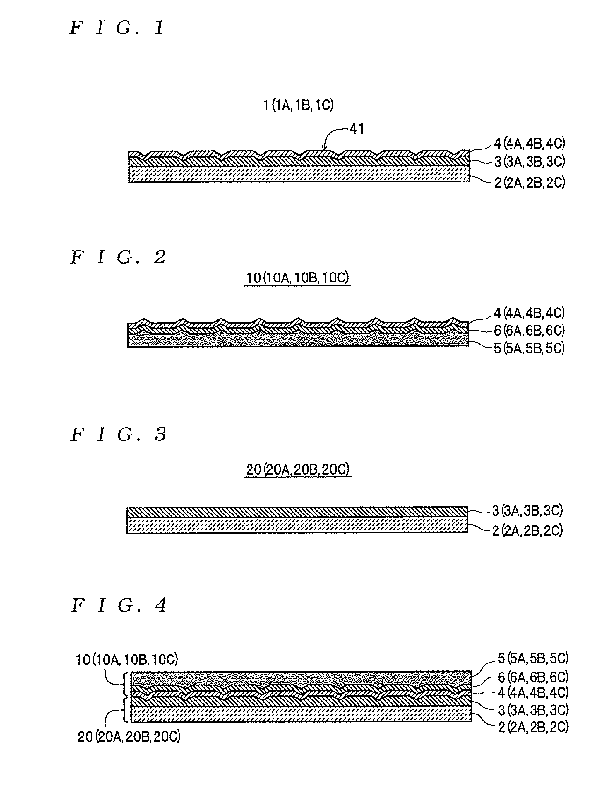
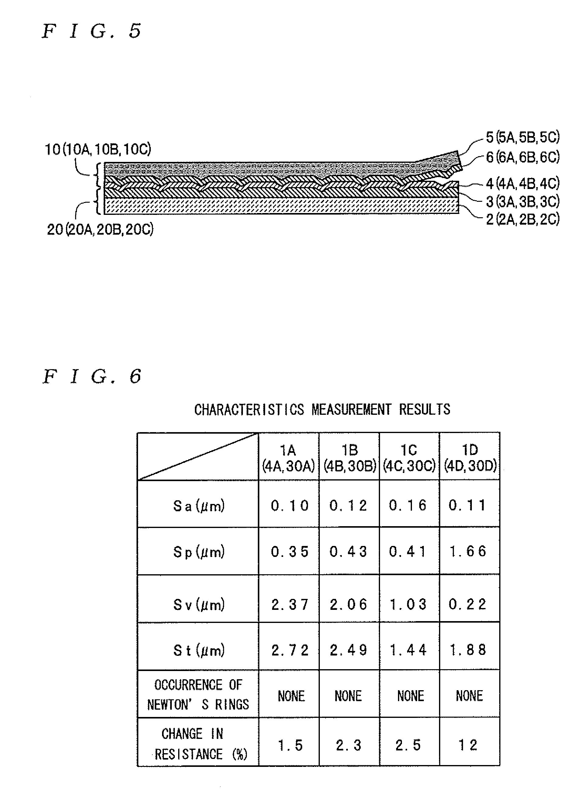
[0027]First, the construction of a transparent conductive film 1 will be described with reference to the drawings.

[0028]The transparent conductive film 1 shown in FIG. 1 is one example of a transparent conductor according to the present invention and includes a support 2, a resin layer 3, and a transparent conductive layer 4. Note that the term “transparent” for the present invention means that visible light can be transmitted and includes a state where some scattering of light occurs. Here, the extent to which light is scattered differs according to the intended use of the transparent conductive film 1, with a level of scattering normally referred to as “semi-transparent” also included in the term “transparent” for the present invention.

[0029]The support 2 is formed in a film-like form or plate-like form using a transparent material...


PUM

PropertyMeasurementUnit
surface roughnessaaaaaaaaaa

Abstract

A transparent conductor includes a film-shaped or plate-shaped support and a transparent conductive layer that is disposed on the support and has a surface formed as a rough surface. The surface of the transparent conductive layer is formed so that a maximum peak height that shows a surface roughness of the surface is in a range of 0.35 μm to 0.43 μm, inclusive.

Description

BACKGROUND OF THE INVENTION[0001]1. Field of the Invention[0002]The present invention relates to a transparent conductor where a transparent conductive layer is disposed on a film-shaped or plate-shaped support.[0003]2. Description of the Related Art[0004]As one example of this type of transparent conductor, a transparent electrode (the outer transparent electrode that is touched) used in a touch panel disclosed by Japanese Laid-Open Patent Publication No. H11-250764 is known. This transparent electrode is constructed of a transparent resin film and a transparent thin-film electrode layer that is laminated on the transparent resin film. To prevent Newton's rings (interference fringes) from being produced when the transparent electrode is touched with a finger or a pen, the surface of the transparent thin-film electrode layer is formed with a surface roughness within a predetermined range. The “center line average roughness” and “maximum height” that show the surface roughness of the...

Claims


Application Information

Patent Timeline
Patent Type & Authority Patents(United States)
IPC IPC(8): H01B11/06
CPCH01L31/1884G02F2001/133776Y02E10/50G02F2203/03G02F1/133776
Inventor YAMADA, CHIEKOKUROSE, SHIGEOHIKIDA, KOICHI
Owner TDK CORPARATION
Why Eureka
Try Eureka