Display panel electrode structure
a technology of electrode structure and display panel, applied in the field of display panel, can solve the problems of high power consumption when representing low gray scale or actual moving, insufficient gap, electric field, etc., and achieve the effect of reducing power consumption and suitable discharg
- Summary
- Abstract
- Description
- Claims
- Application Information
AI Technical Summary
Benefits of technology
Problems solved by technology
Method used
Image

Examples
Embodiment Construction
[0038]Hereinafter, exemplary embodiments of the present invention will be described in detail with reference to the attached drawings.
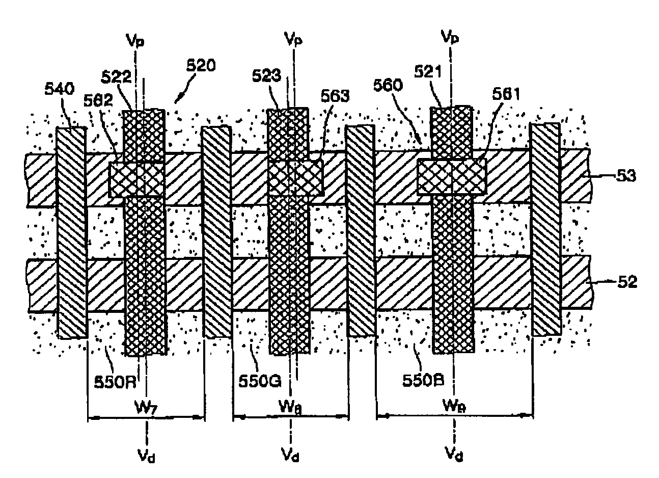
[0039]FIG. 5 is an exploded perspective view of a portion of a PDP 50. Referring to FIG. 5, the PDP 50 includes a front substrate 51 and a rear substrate 510 facing the front substrate 51.
[0040]X and Y electrodes 52 and 53 are alternately arranged as sustaining electrodes 54 at predetermined distances on a lower surface of the front substrate 51. Discharge spaces are formed between the X and Y electrodes 52 and 53. The X and Y electrodes 52 and 53 have a stripe shape, and may be formed of transparent conductive layers. Bus electrodes 55 are formed on lower surfaces of the X and Y electrodes 52 and 53 to reduce a line resistance of the sustaining electrodes 54.
[0041]An area between a pair of adjacent sustaining electrodes 54 corresponds to a non-discharge area, where a black matrix layer may be formed to improve the PDP's contrast.
[0042]A front dielect...
PUM
 Abstract
Description
Claims
Application Information