LTCC-based modular MEMS phased array

a phased array and modular technology, applied in the direction of waveguide type devices, radiating element structural forms, resonance antennas, etc., can solve the problems of substantial structural and functional differences between ic and mems, production costs are still prohibitive for some applications, and the use of ic packaging processes for the manufacture of mems devices, etc., to achieve low cost, reduce thermal and mechanical stresses, and simplify the phased array fabrication process

Inactive Publication Date: 2007-10-30
COMSAT
View PDF7 Cites 27 Cited by
  • Summary
  • Abstract
  • Description
  • Claims
  • Application Information

AI Technical Summary

Benefits of technology

[0013]It is another object of the present invention to provide a low-cost, efficient method of fabricating a phased array with MEMS technology.
[0014]It is still another object of the present invention to simplify the phased array fabrication process by using LTCC technology to manufacture substantially all layers of the phased array. The use of same or similar material for all the layers in the subarray structure reduces the thermal and mechanical stresses that may result from using dissimilar materials of different coefficients of thermal expansion.

Problems solved by technology

PCT / US02 / 03379 reduces the cost of making the active phased arrays due to the modularity of the design and the use of lower loss MEMS components, the production costs are still prohibitive for some applications.
For example, but not by way of limitation, it is a disadvantage of the related art MEMS fabrication process that IC packaging processes must be used for manufacture of MEMS devices.
As noted above, there are substantial structural and functional differences between IC and MEMS, including the need for MEMS to be manufactured in substantially continuous and intimate contact with their environment.
Thus, the related art MEMS fabrication process is not efficient
Further, in the related art, a new, specialized package must be created each time a new MEMS device is developed, at an additional time and financial cost.
As a result, the related art MEMS fabrication process has another disadvantage and is one of the most expensive aspects of MEMS product development, as there are no related art standardized packages from which one would be able to choose a MEMS package for a new application without substantially compromising performance.
Also, the related art fabrication process has another disadvantage, due to its complexity, and requires a substantial research investment to generate a suitable fabrication sequence.
Because the design is dependent on the fabrication, there is an additional cost in that process-independent design tools cannot be used by a MEMS designer.

Method used


Image

  • LTCC-based modular MEMS phased array
  • LTCC-based modular MEMS phased array
  • LTCC-based modular MEMS phased array

Examples


Embodiment Construction

[0022]Reference will now be made in detail to an illustrative, non-limiting embodiment of the present invention, examples of which are illustrated in the accompanying drawings. In the present invention, the terms are meant to have the definition provided in the specification, and are otherwise not limited by the specification.

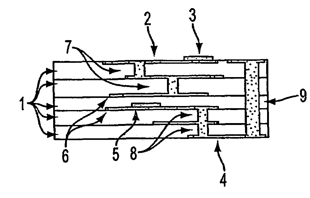
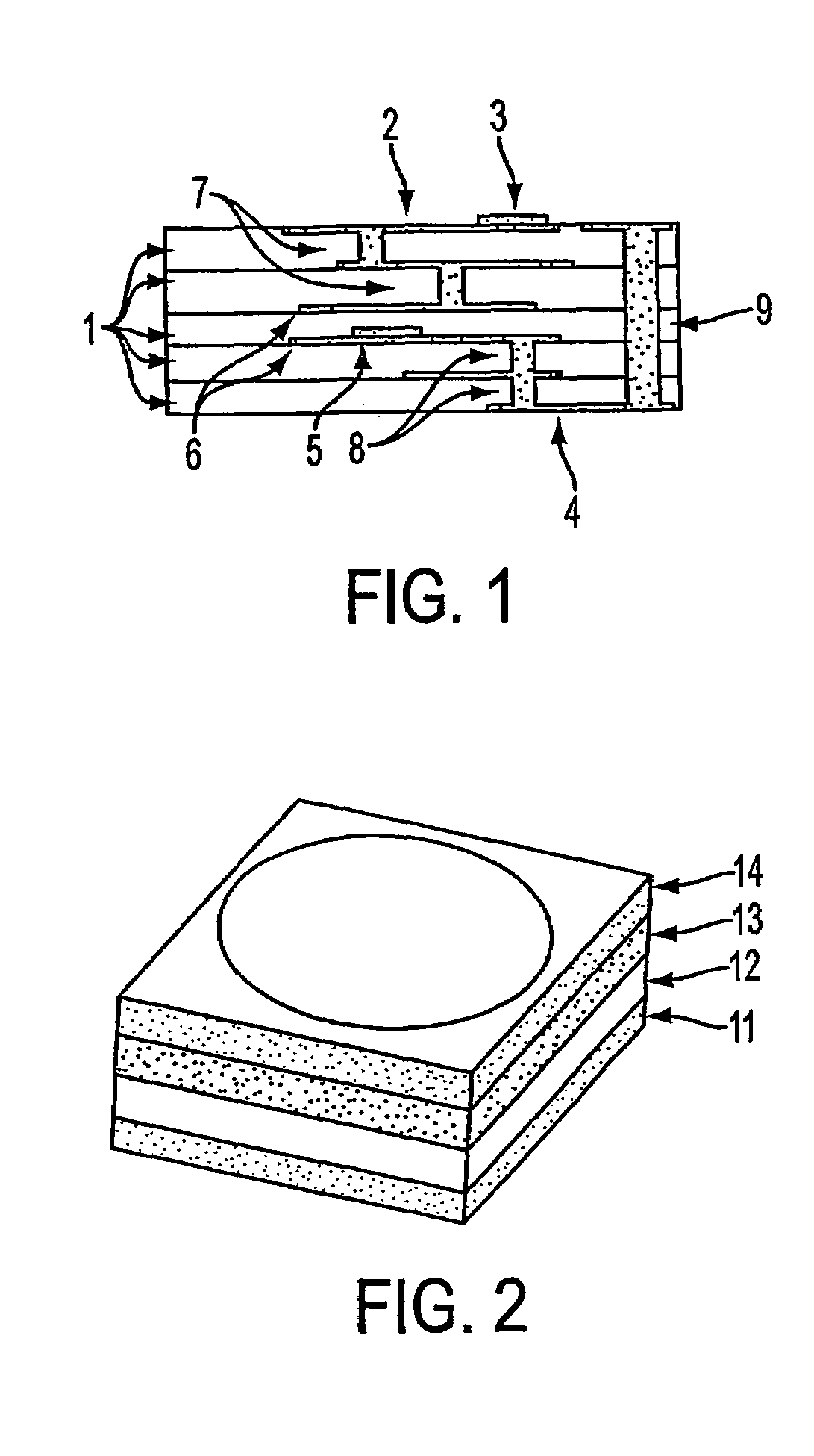
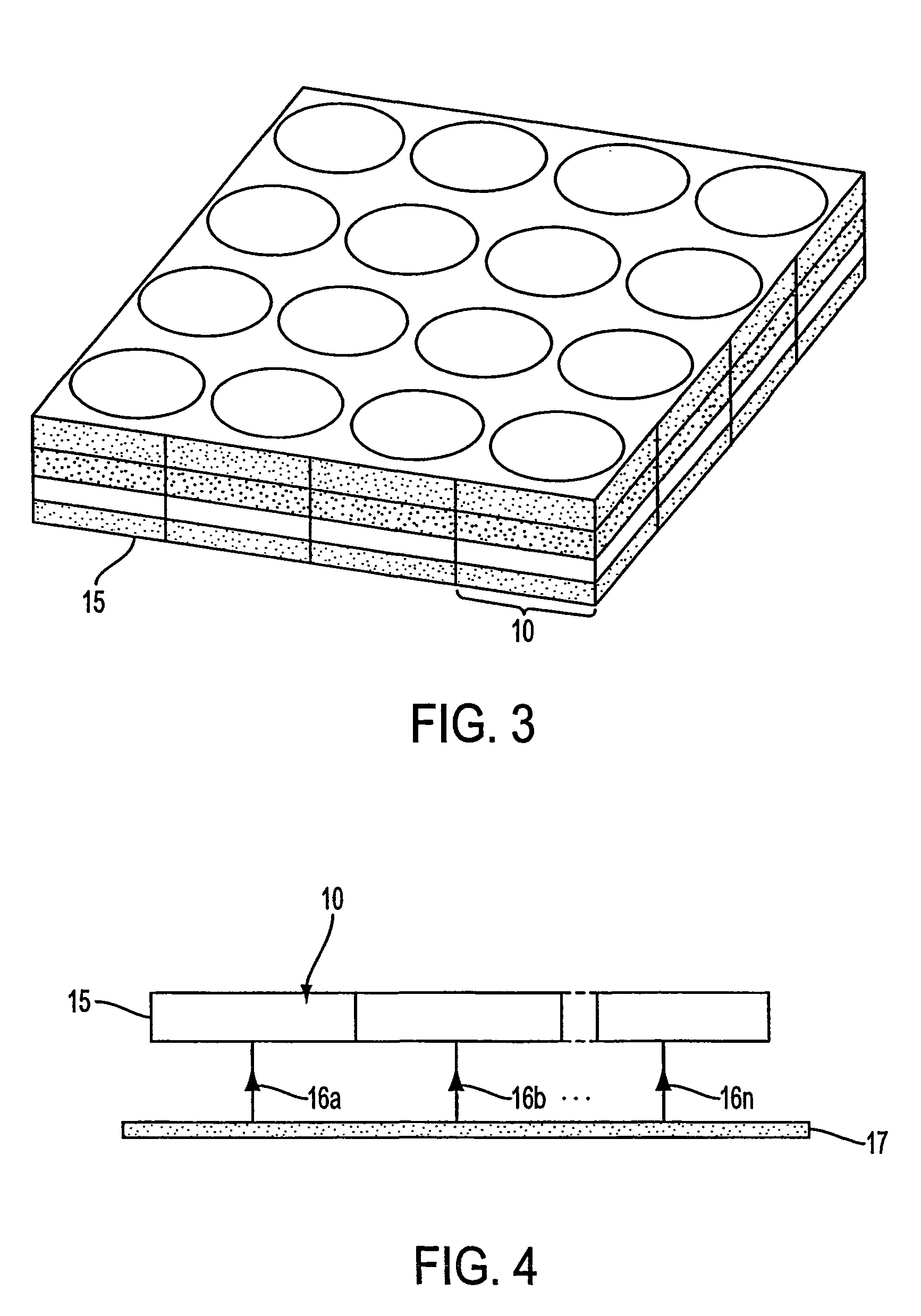
[0023]The present invention relates to a low cost phased array that is constructed using building blocks of subarray modules built in low temperature co-fired ceramic material (LTCC). The modules are highly integrated to include radiating elements and other components including, but not limited to phase shifters, polarizing circuits and filters. Each module includes a subarray of radiating elements and a number of electronic components that may include polarization circuits, phase shifters, power divider networks, and / or filters. The various components in the different layers are integrated together via vertical interconnects (e.g., vias) by using the LTCC mate...


PUM

PropertyMeasurementUnit
temperatureaaaaaaaaaa
frequenciesaaaaaaaaaa

Abstract

The present invention uses low temperature co-fired ceramic (LTCC) technology for fabrication of micro-electro-mechnical systems (MEMS) based phase shifters. As a result, low-cost subarray modules can be constructed using LTCC, and the subarray modules (10) can be used as building blocks for large antenna arrays. In an exemplary description of the present invention, all layers of the multilayer subarray modules, including MEMS, are in LTCC. As a result, a significant cost reduction for satellite terminals using highly integrated LTCC subarray modules.

Description

[0001]This application claims the benefit of U.S. Provisional Application No. 60 / 283,915, filed Apr. 13, 2001, under 35 U.S.C. § 119(e).BACKGROUND OF THE INVENTION[0002]1. Field of the Invention[0003]The present invention relates to a method of efficiently fabricating a low-cost phased array. More specifically, the present invention relates to a multilayer phased array and method of fabrication thereof, using low temperature co-fired ceramic (LTCC)— based layers, some of which are micro-electromechanical system (MEMS) layers.[0004]2. Background of the Invention[0005]In the related art, micro-electromechanical system (MEMS) technology integrates the silicon substrate of printed-circuit and computer technologies with tiny mechanical devices. For example, but not by way of limitation, MEMS technology may include sensors, valves, gears, mirrors, switches or actuators embedded in semiconductor devices.[0006]While the related art electronics of MEMS devices are fabricated via an Integrate...

Claims


Application Information

Patent Timeline
Patent Type & Authority Patents(United States)
IPC IPC(8): H01Q1/38H04Q1/38
CPCB81C1/00253Y10T29/49018Y10T29/49016
Inventor ZAGHLOUL, AMIR I.
Owner COMSAT
Why Eureka
Try Eureka