Thin film transistor substrate and production method thereof

a technology of thin film transistors and substrates, applied in the direction of instruments, semiconductor devices, electrical devices, etc., to achieve the effect of preventing damag

Active Publication Date: 2007-11-06
SHARP KK
View PDF6 Cites 2 Cited by
  • Summary
  • Abstract
  • Description
  • Claims
  • Application Information

AI Technical Summary

Benefits of technology

[0019]An object of the present invention is to provide (i) a thin film transistor substrate including a peripheral circuit capable of preventing damage on a characteristic of a thin film transistor in a polycrystallization process and (ii) a method for producing the thin film transistor substrate.
[0020]Further, an object of the present invention is to provide a thin film transistor substrate capable of maintaining a desired characteristic of a thin film transistor even when a peripheral circuit area is defined on an extended portion of a stripe area where TFTs of a display area are disposed in a line and then a thin film transistor is formed on the extended portion.
[0024]When an area is polycrystallized by scanning of laser light in a certain direction and then receives irradiated laser light scanning in another direction, crystal characteristics are out of order and a characteristic of a thin film transistor is damaged. Currently, it is difficult to minutely control where to irradiate laser light in a scanning direction. However, with the foregoing arrangements, a channel requested to have a desired characteristic is positioned on a portion other than a portion where crystal characteristics may be out of order, with a result that it is possible to reduce the influence of disorders of crystal characteristics.
[0025]Further, when a semiconductor film is polycrystallized twice, second polycrystallization has a greater influence on the characteristic of the semiconductor film. Therefore, by polycrystallizing the peripheral circuit area after the display area, it becomes easy to secure a TFT characteristic of the peripheral circuit area.

Problems solved by technology

In a case of forming a thin film transistor (TFT) on a glass substrate, an amorphous silicon film was used because heat-resistant temperature of the glass substrate is limited.

Method used


Image

  • Thin film transistor substrate and production method thereof
  • Thin film transistor substrate and production method thereof
  • Thin film transistor substrate and production method thereof

Examples


first embodiment

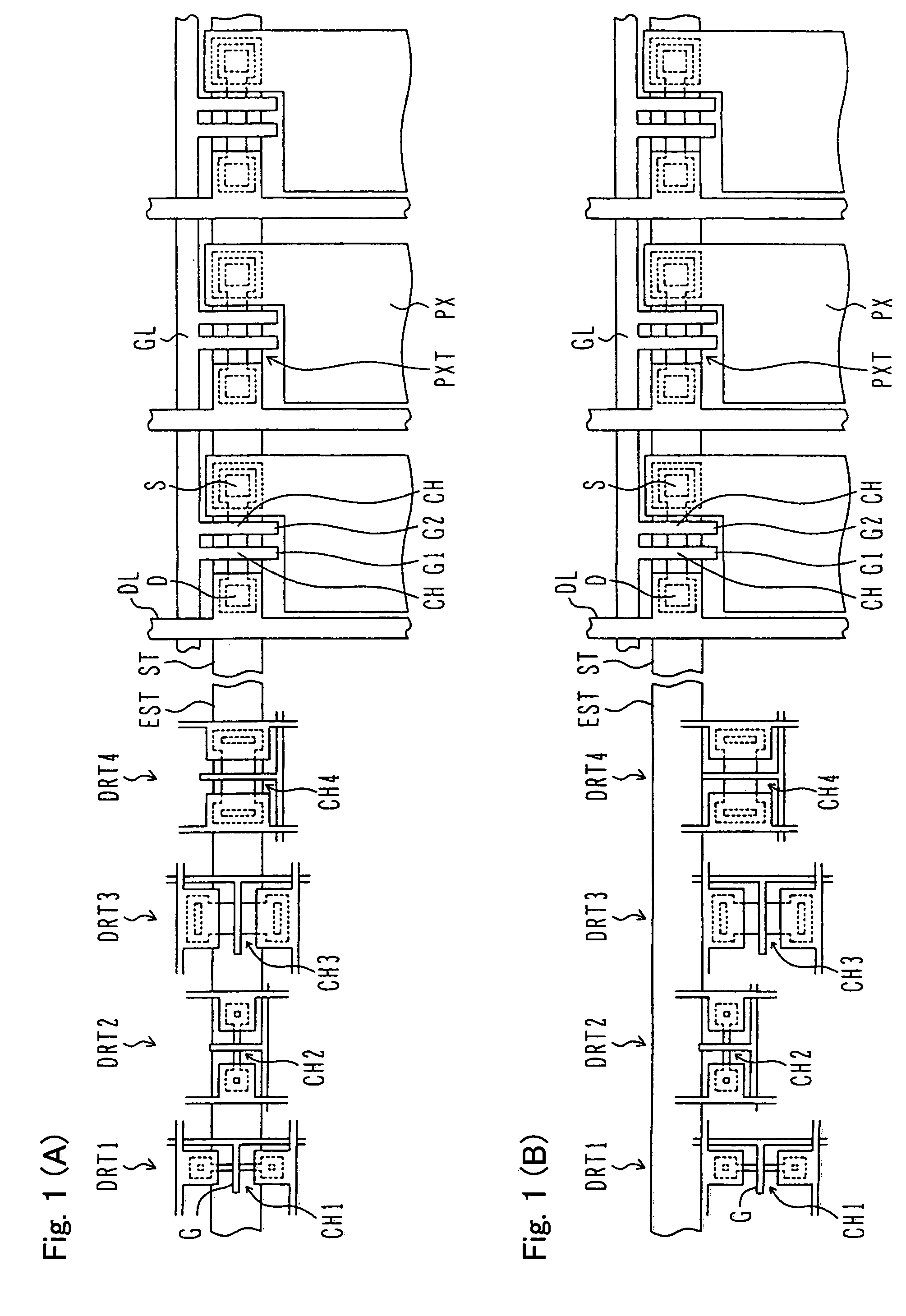
[0050]FIGS. 1(A) and 1(B) are plan views illustrating structures of thin film transistor substrates according to the present invention.

[0051]FIG. 1(A) illustrates a structure of a thin film transistor substrate without any arrangement for avoiding the damage on the characteristic of a TFT. A display area is illustrated at a right side of FIG. 1(A) and a gate side driving circuit is illustrated at a left side of FIG. 1(A). In the display area, pixels are disposed in a matrix manner, a gate line GL is disposed in line with each pixel row and a drain line DL is disposed in line with each pixel column. A pixel thin film transistor PXT is disposed at a left-upper corner of each pixel.

[0052]The pixel thin film transistor PXT includes a drain D connected with the drain line, a source S connected with a pixel electrode PX, double gates G 1 and G 2 connected with the gate line GL, and a channel CH under a gate. A channel length direction is a horizontal row direction.

[0053]In the gate side d...

second embodiment

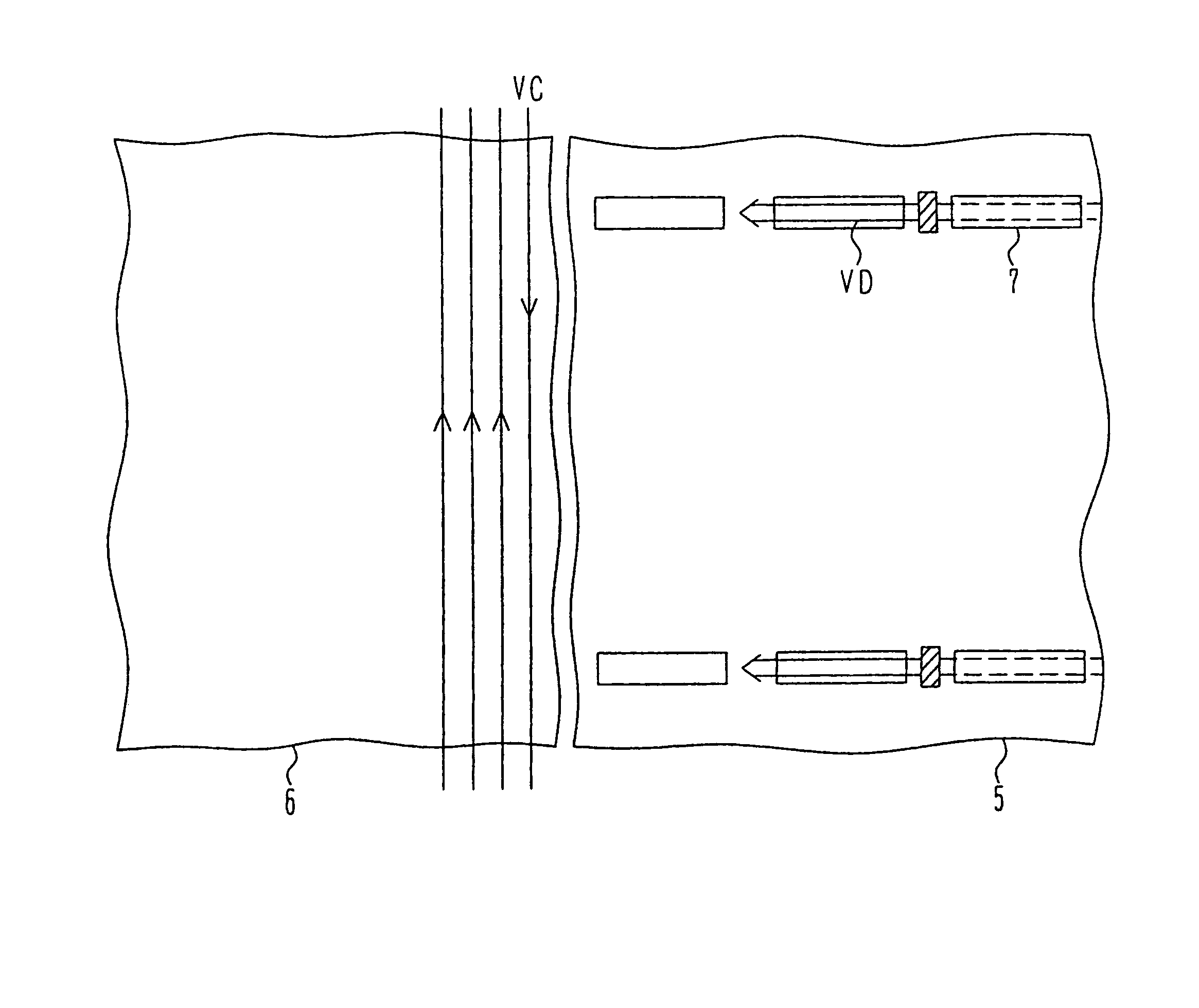
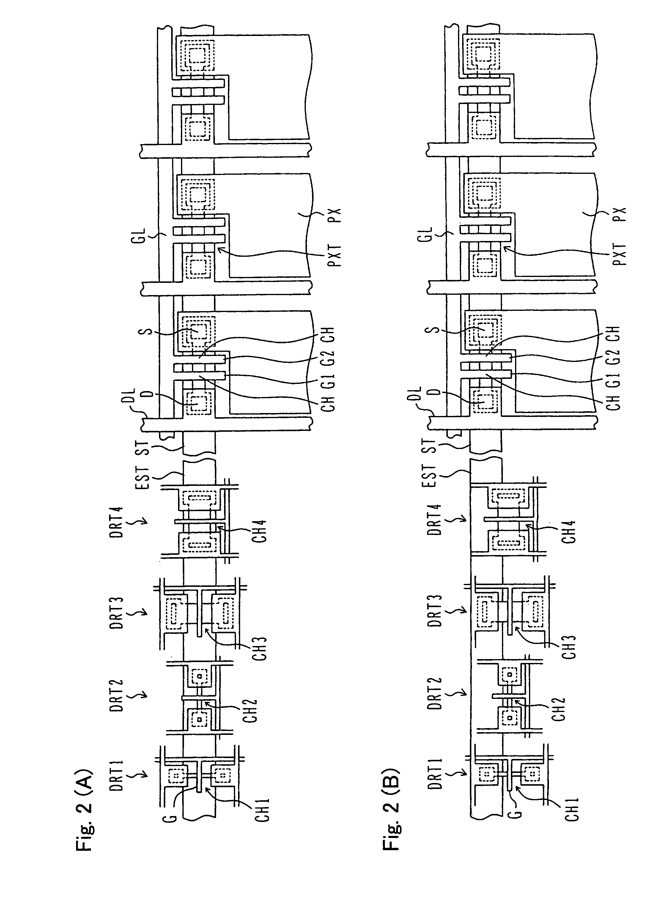
[0057]FIGS. 2(A) and 2(B) are plan views illustrating structures of thin film transistor substrates according to the present invention. FIG. 2(A) illustrates initial disposition that is likely to be subject to the damage as with FIG. 1(A). FIG. 2(B) illustrates disposition of TFTs in which a channel having an influence on an ability of a transistor is displaced out of the extended portion EST of the laser light irradiation stripe area ST. As long as the channel is not damaged, even when the source S and the drain D having high density of impurity receives irradiated laser light in different scanning directions, there is little influence on the characteristic of the transistor. Because the TFT is displaced in consideration of only the channel, it is possible to reduce the limitation on the design. Particularly, it is possible to reduce amounts of displacements of the thin film transistors DRT 1 and DRT 3 having the channel length directions in a vertical direction.

[0058]The foregoing...


PUM


Abstract

A method for producing a thin film transistor substrate includes the steps of: (i) depositing an amorphous semiconductor film on a transparent insulating substrate; (ii) patterning the amorphous semiconductor film so as to form insular amorphous semiconductor films, the step (ii) including a process (I) for forming, in respective stripe areas each of which is elongate in a first direction in a display area, a plurality of insular semiconductor films whose channel length is in line with the first direction, and a process (II) for forming, in an area including extended portions of the striped areas in a peripheral circuit area, a plurality of insular semiconductor films; (iii) polycrystallizing the insular semiconductor films in the peripheral circuit area so that the insular semiconductor films have high mobility in a second direction and polycrystallizing the insular semiconductor films in the display area so that the insular semiconductor films have high mobility in the first direction; and (iv) forming TFTs by using polycrystalline insular semiconductor films. In at least one peripheral circuit, a channel of a high speed TFT is positioned on a portion other than the extended portions of the stripe areas.

Description

[0001]This non-provisional application claims priority under 35 U.S.C. § 119(a) on Patent Application No. 2005-81967 filed in Japan on Mar. 22, 2005, the entire contents of which are hereby incorporated by reference.FIELD OF THE INVENTION[0002]The present invention relates to a thin film transistor substrate having a thin film transistor and to a method for producing the thin film transistor substrate. The present invention particularly relates to a thin film transistor substrate using a polycrystalline silicon thin film and to a method for producing the thin film transistor substrate.BACKGROUND OF THE INVENTION[0003]Recently, a liquid crystal display device or an organic EL display device has been often used as a flat panel display. By using an active matrix substrate in which a switching (active) element such as a thin film transistor (TFT) is formed so as to correspond to each display pixel, it is possible to enhance an ability of a display device. Such active matrix substrate is...

Claims


Application Information

Patent Timeline
Patent Type & Authority Patents(United States)
IPC IPC(8): H01L29/76
CPCH01L27/12H01L27/1285H01L29/04G02F1/13454
Inventor HOTTA, KAZUSHIGEHIRANO, TAKUYA
Owner SHARP KK
Why Eureka
Try Eureka