Moving head for semiconductor wafer polishing apparatus

a polishing apparatus and moving head technology, applied in the direction of grinding drives, manufacturing tools, lapping machines, etc., can solve the problems of reducing surface roughness, affecting polishing function, and affecting polishing accuracy, so as to achieve precise final polishing

Inactive Publication Date: 2007-11-13
INHA UNIV RES & BUSINESS FOUNDATION
View PDF6 Cites 18 Cited by
  • Summary
  • Abstract
  • Description
  • Claims
  • Application Information

AI Technical Summary

Benefits of technology

[0013]Accordingly, the present invention has been made keeping in mind the above problems occurring in the prior art, and the present invention relates to the polishing of a semiconductor wafer material from which an integrated circuit is made. That is, an object of the present invention is to provide a moving head for semiconductor wafer polishing apparatuses, which detects vibrations transmitted to a wafer and outputs signals indicating frictional force and pressing force acting on the wafer, using a load cell and a piezoelectric sensor installed in the moving head so as to maintain optimum frictional force and pressing force relative to the surface of a polishing pad, thus realizing precise final polishing.

Problems solved by technology

However, due to the special characteristics of wafers, the results of most of the research are not clear.
However, as the final polishing process is continuously performed, the surface roughness is reduced, and thus a polishing function is gradually lost.
However, when the pad conditioning operation is conducted, the pad conditioner is repeatedly used without checking the condition of the polishing pad using a sensor.
Thus, it is impossible to know the condition of the pad.
The method is problematic in that dressing is required every time a polishing process is conducted without monitoring frictional force or pressing force, so that the efficiency of the process is low.
In other words, the frictional force of the moving head in the CMP apparatus is detected at the exterior, and thus the detected result may be slightly inaccurate due to factors interfering with the detection.
However, the conventional wafer polishing apparatus is problematic in that it is impossible to monitor frictional force and pressing force, which are important factors affecting surface roughness in the final wafer polishing process, in real time, and thus the efficiency of polishing the wafer is poor.

Method used


Image

  • Moving head for semiconductor wafer polishing apparatus
  • Moving head for semiconductor wafer polishing apparatus
  • Moving head for semiconductor wafer polishing apparatus

Examples


Embodiment Construction

[0021]Hereinafter, the preferred embodiment of the present invention will be described in detail with reference to the accompanying drawings.

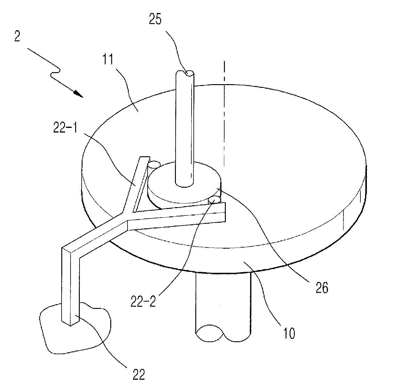
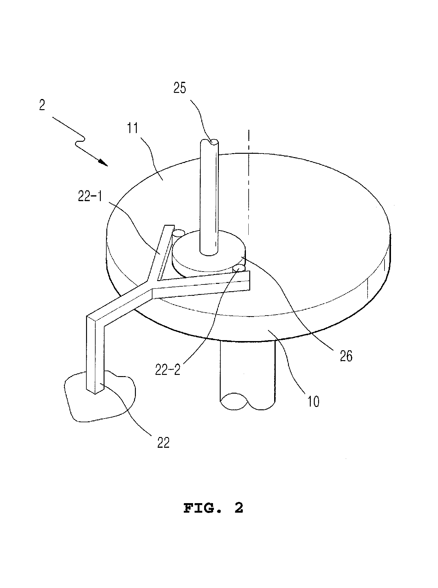
[0022]FIG. 2 is a view schematically showing a semiconductor wafer polishing apparatus equipped with a moving head, according to the present invention, and FIG. 3 is a side sectional view showing the moving head of FIG. 2.

[0023]Referring to the drawings, a semiconductor wafer polishing apparatus 2 includes a table 10 and a moving head 20. A polishing pad 11 is formed on the table 10. The moving head 20 is mounted on the polishing pad 11, and brings a wafer 21 into close contact with the surface of the polishing pad 11 of the table 10 via a support unit 22.

[0024]A load cell 23 and a piezoelectric sensor 24, which are sensing means, are provided in the moving head 20, and measure pressing force and frictional force acting on the wafer 21 provided inside the moving head 20.

[0025]The moving head 20 is connected to branch rods 22-1 of the support un...


PUM


Abstract

Disclosed herein is a moving head for a semiconductor wafer polishing apparatus. The semiconductor wafer polishing apparatus has a table on which a polishing pad is formed, and the moving head mounted via a support unit to hold a wafer relative to a polishing surface of the table. In this case, the moving head includes a sensing means having a load cell and a piezoelectric sensor to measure pressing force and frictional force acting on the wafer provided in the moving head. The present invention relates to the polishing of a semiconductor wafer material from which an integrated circuit is made. That is, the present invention provides a moving head for semiconductor wafer polishing apparatuses, which detects vibrations transmitted to a wafer and outputs signals indicating frictional force and pressing force acting on the wafer, using a load cell and a piezoelectric sensor installed in the moving head so as to maintain optimum frictional force and pressing force relative to the surface of a polishing pad, thus realizing precise final polishing.

Description

BACKGROUND OF THE INVENTION[0001]1. Field of the Invention[0002]The present invention relates generally to a moving head for semiconductor wafer polishing apparatuses and, more particularly, to the polishing of a semiconductor wafer material from which an integrated circuit is made. That is, the present invention relates to a moving head for semiconductor wafer polishing apparatuses, which detects vibrations transmitted to a wafer and outputs signals indicating frictional force and pressing force acting on the wafer, using a load cell and a piezoelectric sensor installed in the moving head so as to maintain optimum frictional force and pressing force relative to the surface of a polishing pad, thus realizing precise final polishing.[0003]2. Description of the Related Art[0004]Generally, since a wafer polishing process is a process for realizing final flatness and surface roughness, prior to a device assembly process, the wafer polishing process is very important. Because it is so im...

Claims


Application Information

Patent Timeline
Patent Type & Authority Patents(United States)
IPC IPC(8): B24B49/00B24B37/04
CPCB24B37/005B24B49/16B24B49/10B24B37/04H01L21/304
Inventor LEE, EUN SANGWON, JONG GOOLEE, JUNG TALK
Owner INHA UNIV RES & BUSINESS FOUNDATION
Why Eureka
Try Eureka