Method for manufacturing diffraction optical element
- Summary
- Abstract
- Description
- Claims
- Application Information
AI Technical Summary
Benefits of technology
Problems solved by technology
Method used
Image

Examples
example 1
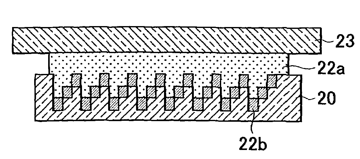
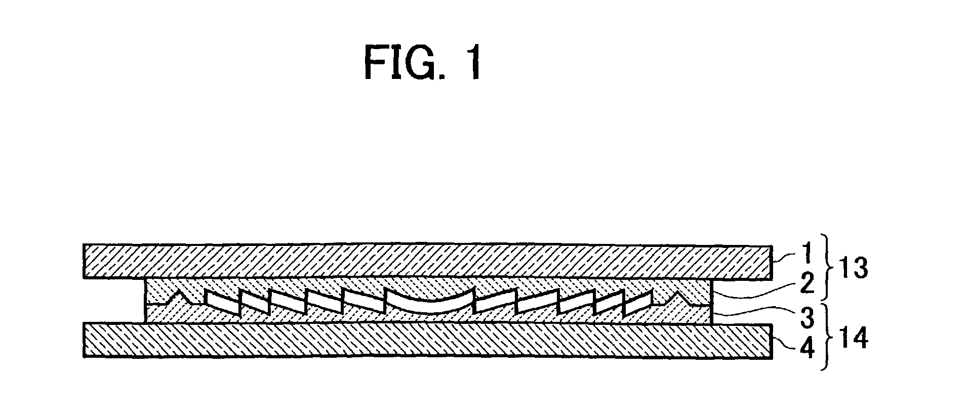
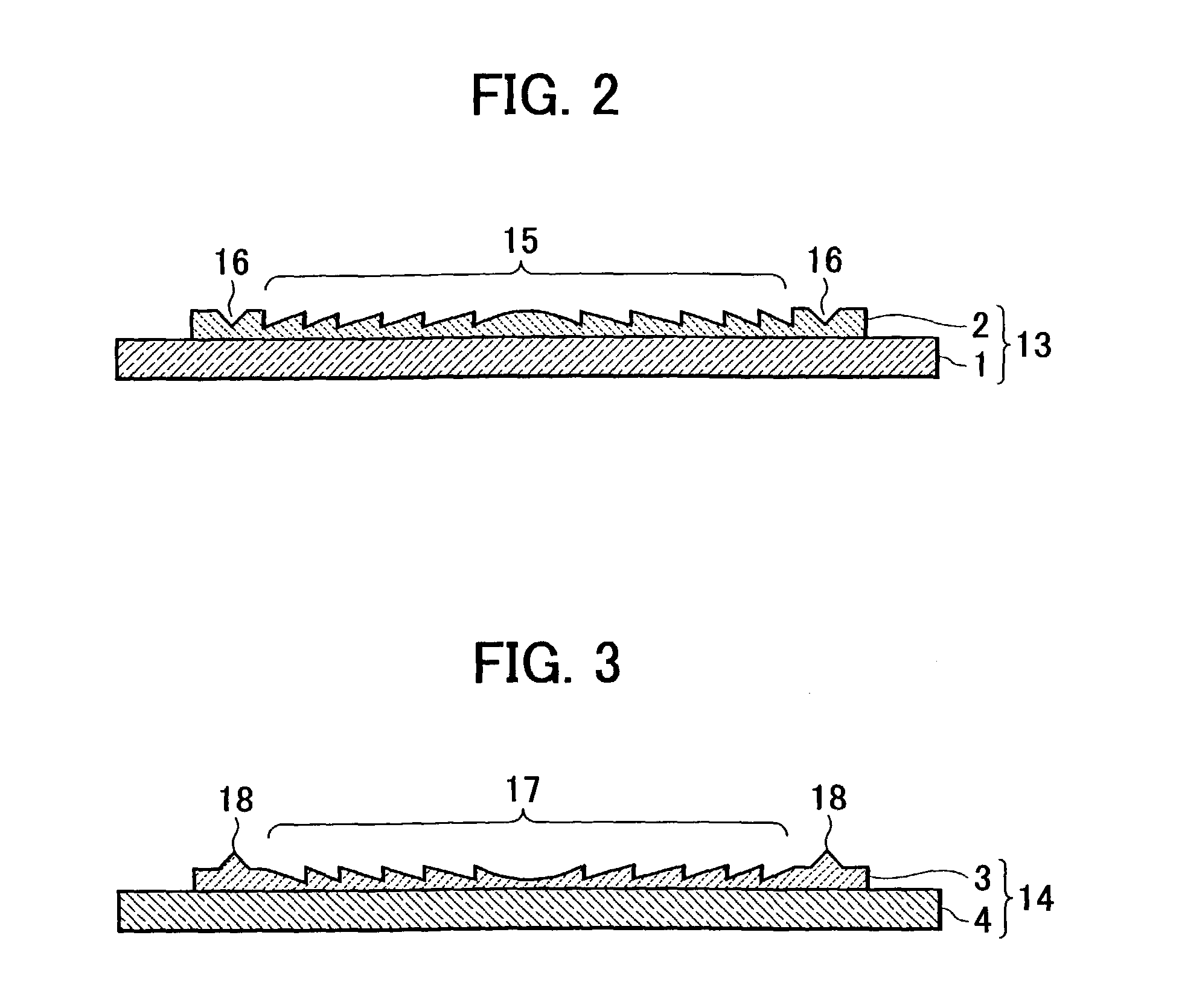
[0031]One example of a manufacturing method of the diffraction optical element, according to present invention, will be described with reference to FIGS. 5, and 8A to 8D. FIGS. 8A to 8D are views each showing only the glass substrate, the photocurable resin, and the molding die among the various elements shown in FIG. 5 for illustrating a curing process of a photocurable resin. In FIGS. 8A to 8D, the same reference numerals as those in FIG. 5 designate the same elements, and a detailed description thereof is omitted.
[0032]First, the support frame 21 was fitted to the molding die 20 shown in FIG. 5. A predetermined amount of the photocurable resin 22 was dripped onto the mold surface of this molding die 20 by using a dispenser not shown in the figure. After this photocurable resin 22 spread over the entire mold surface, a vacuum device, in which the molding apparatus shown in FIG. 5 was placed, was evacuated to approximately 10 mm Hg for defoaming. When the grating shape has a pitch ...
example 2
[0043]A diffraction optical element was formed in the same manner as that in Example 1, except that the photocurable resin used in Example 1 was replaced with a photocurable resin that allowed light having a short wavelength (300 nm) to pass therethrough to some extent. In this example, in order to improve ultraviolet-ray absorption properties of the photocurable resin, an ultraviolet ray absorber (stabilizer) was added thereto. Since the photocurable resin used in this example was a urethane acrylate-based material, by adding a triazine-based ultraviolet ray absorber sold under the registered trade-name TINUVIN 400 by Ciba Specialty Chemicals Corporation, a resin having a large absorption spectrum for light having a wavelength of 346 nm or less can be obtained. In this example, a diffraction optical element having superior structural accuracy can also be manufactured.
[0044]In addition to the examples described above, the present invention can be modified in various ways. For exampl...
PUM
| Property | Measurement | Unit |
|---|---|---|
| Wavelength | aaaaa | aaaaa |
| Wavelength | aaaaa | aaaaa |
Abstract
Description
Claims
Application Information
 - R&D Engineer
- R&D Manager
- IP Professional
- Industry Leading Data Capabilities
- Powerful AI technology
- Patent DNA Extraction
Browse by: Latest US Patents, China's latest patents, Technical Efficacy Thesaurus, Application Domain, Technology Topic.
© 2024 PatSnap. All rights reserved.Legal|Privacy policy|Modern Slavery Act Transparency Statement|Sitemap