Micro-lens built-in vertical cavity surface emitting laser
- Summary
- Abstract
- Description
- Claims
- Application Information
AI Technical Summary
Benefits of technology
Problems solved by technology
Method used
Image

Examples
first embodiment
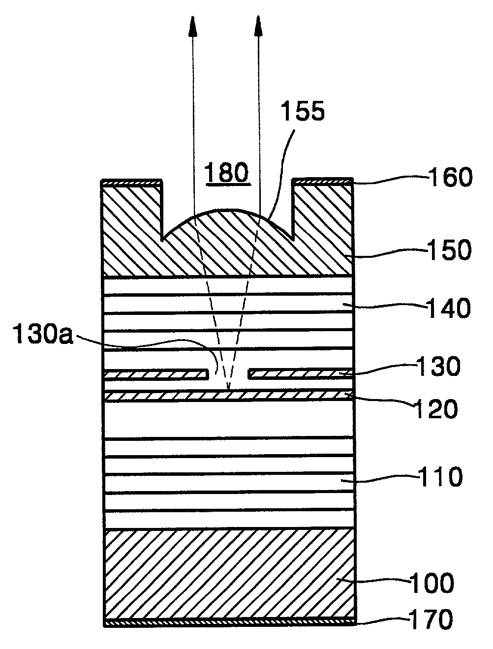
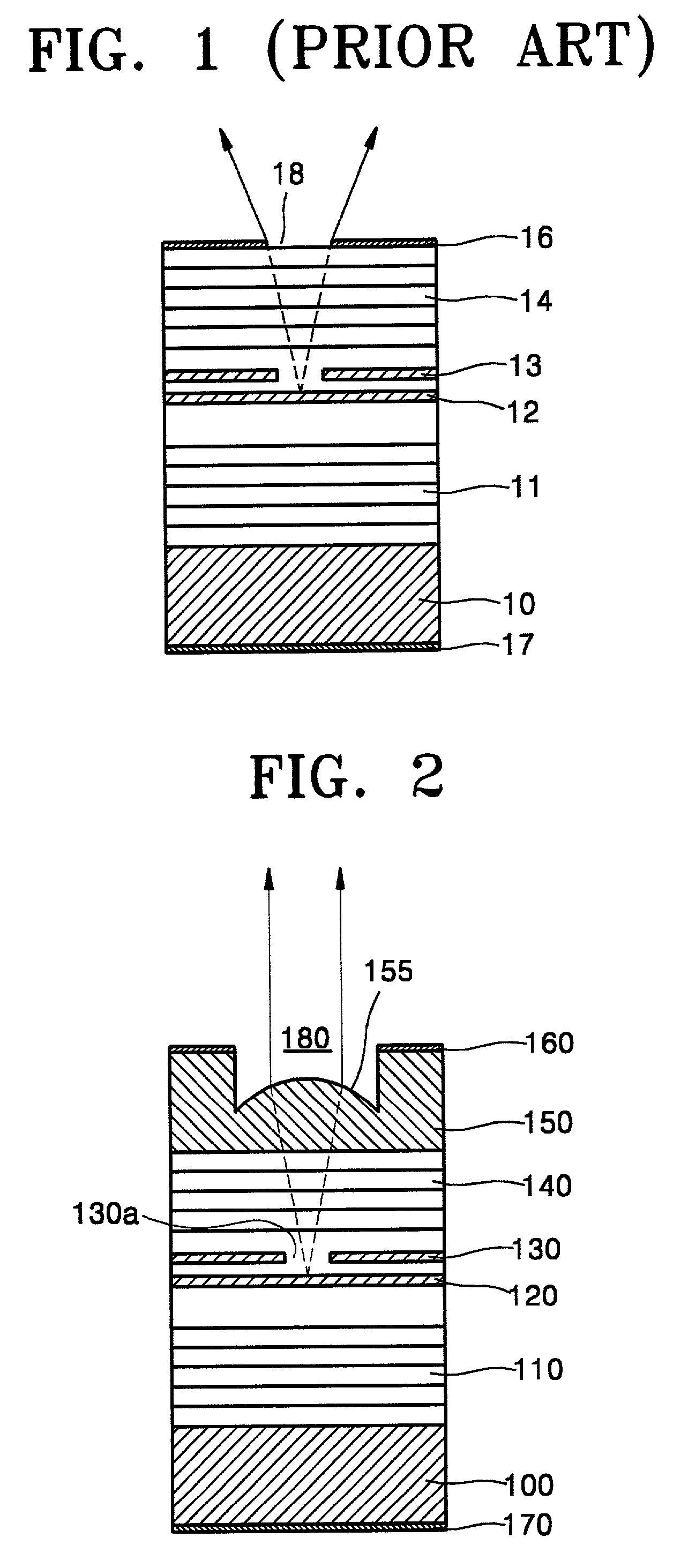
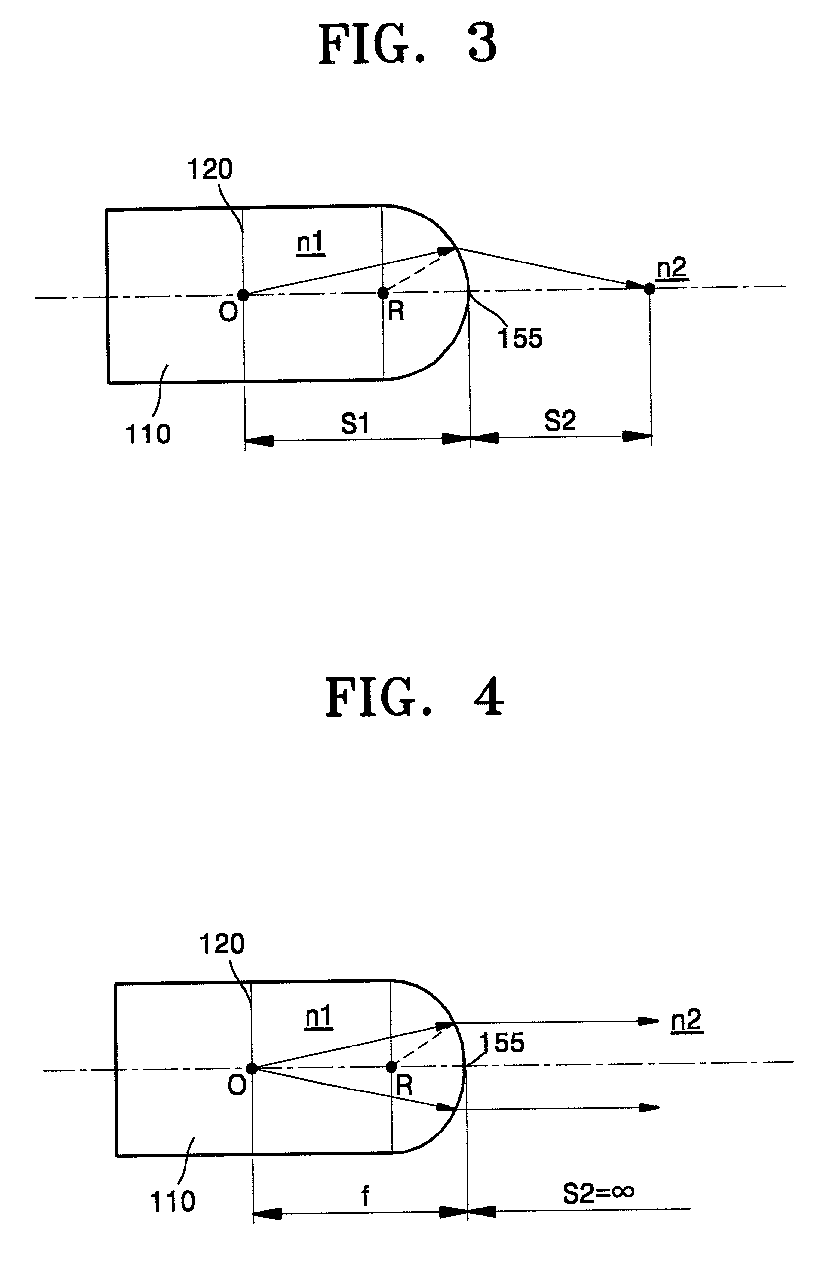
[0035]As described above, when the VCSEL, according to the present invention, is designed such that the light is generated in a region as small as possible on the active layer 120, the light generating region may be ideally a dot-sized region. In this case, the light going toward the lens layer 150 from the light generating region is approximately diverging light originating from the dot-sized light generating region.
[0036]The lens layer 150 has a predetermined thickness, for example, of several micrometers and may be deposited on the upper reflector 140. For instance, the lens layer 150 is formed of a material having a relatively wide bandgap to the wavelength of the laser beam generated from the VCSEL, so as not to absorb, but transmit and emit the laser beam through the upper reflector 140. In addition, when the lens layer 150 is formed directly on the upper reflector 140, the lens layer 150 may be formed of a material capable of lattice matching with the material of the upper re...
second embodiment
[0051]Referring to FIG. 5, the micro-lens built-in VCSEL, according to the present invention, includes a substrate 200, a lower reflector 210, an active layer 120, and an upper reflector 240 which are sequentially stacked on the substrate 200, an upper electrode 260 formed on the upper reflector 240, and a lower electrode 270 formed on a portion of the bottom of the substrate 200 excluding a window region 280 through which a laser beam is emitted. To emit a laser beam through the substrate 200, the lower reflector 210 is formed having a smaller reflectivity than the upper reflector 240.
[0052]When a number of stacked layers of the lower reflector 210 is smaller than that of the upper reflector 240, the reflectivity of the lower reflector 210 is lower than that of the upper reflector 240. Accordingly, most of the laser beam is emitted through the lower reflector 210. Except for a number of stacked layers of each of the upper and lower reflectors 240 and 210, materials used for and the...
third embodiment
[0057]FIG. 6 shows the micro-lens built-in VCSEL according to the present invention. In FIG. 6, the same reference numerals as those of FIG. 2 represent elements having the same functions as or similar functions to corresponding elements of FIG. 2; thus, descriptions of the elements are not provided here.
[0058]The micro-lens built-in VCSEL, according to the third embodiment of the present invention, includes a window 380 having a diameter (D) satisfying a Fraunhofer diffraction condition. Here, the Fraunhofer diffraction of the window 380 is offset by a focusing power of the micro-lens 355 such that a parallel laser beam is emitted through the micro-lens 355.
[0059]In this case, for instance, a relation between a diameter D of the window 380 and the focal length f of the micro-lens 355 satisfies formula (3):
[0060]D=2×1.22λf(3)
where λ is the wavelength of the laser beam emitted from the VCSEL according to the third embodiment of the present invention.
[0061]The diameter D of the win...
PUM
 Abstract
Description
Claims
Application Information
 - R&D Engineer
- R&D Manager
- IP Professional
- Industry Leading Data Capabilities
- Powerful AI technology
- Patent DNA Extraction
Browse by: Latest US Patents, China's latest patents, Technical Efficacy Thesaurus, Application Domain, Technology Topic.
© 2024 PatSnap. All rights reserved.Legal|Privacy policy|Modern Slavery Act Transparency Statement|Sitemap