Solid-state image sensing element and its design support method, and image sensing device

a technology of image sensing element and design support method, which is applied in the direction of radioation control device, television system, instruments, etc., can solve the problems of light rays not being able to enter the photoelectric conversion unit, phenomenon posing severe bottlenecks, and frame periphery often becoming dark, so as to improve the degree of design freedom and high light collecting efficiency

Active Publication Date: 2006-10-10
CANON KK
View PDF35 Cites 103 Cited by
  • Summary
  • Abstract
  • Description
  • Claims
  • Application Information

AI Technical Summary

Benefits of technology

[0031]The present invention has been made in consideration of the above situation, and has as its first object to provide a solid-state image sensing element which can improve the degree of freedom in design of an image sensing system in an image sensing device, and has high light collecting efficiency according to each image sensing device.
[0032]It is the second object of the present invention to obtain a high-quality image by improving the light collecting efficiency of an image sensing element in an image sensing device having an image sensing lens with a zoom function or focus adjustment function.
[0033]It is the third object of the present invention to realize a digital camera system which can obtain a high-quality image and can obtain a high-resolution image by reducing the size of each pixel in a lens-exchangeable digital camera system.

Problems solved by technology

However, when the condition of the exit pupil of the image sensing lens changes, light rays cannot enter the photoelectric conversion unit and the frame periphery often becomes dark.
Especially, when an image sensing lens that has a zoom function and focus adjustment function is used, the phenomenon poses severe bottlenecks.
However, boosting a signal level to an appropriate level by applying electrical gain is to enhance not only signal components but also noise components, resulting in a low-quality image in which noise is conspicuous on the darkening-corrected peripheral portion.
In case of the conventional compact digital camera, the type of its image sensing system is limited.
That is, in case of the compact digital camera using the conventional solid-state image sensing element, since its image sensing system is limited to a retrofocus system, the degree of freedom in design of the image sensing system drops, and a size reduction of the image sensing system is disturbed.
As a result, light cannot be sufficiently collected on the photoelectric conversion unit.
However, when limb darkening due to the exchangeable lens is large and the output of the image sensing element is small, gain adjustment must be done at a higher gain.
As a result, noise components are also amplified, and a high-quality image signal cannot be obtained.

Method used


Image

  • Solid-state image sensing element and its design support method, and image sensing device
  • Solid-state image sensing element and its design support method, and image sensing device
  • Solid-state image sensing element and its design support method, and image sensing device

Examples


first embodiment

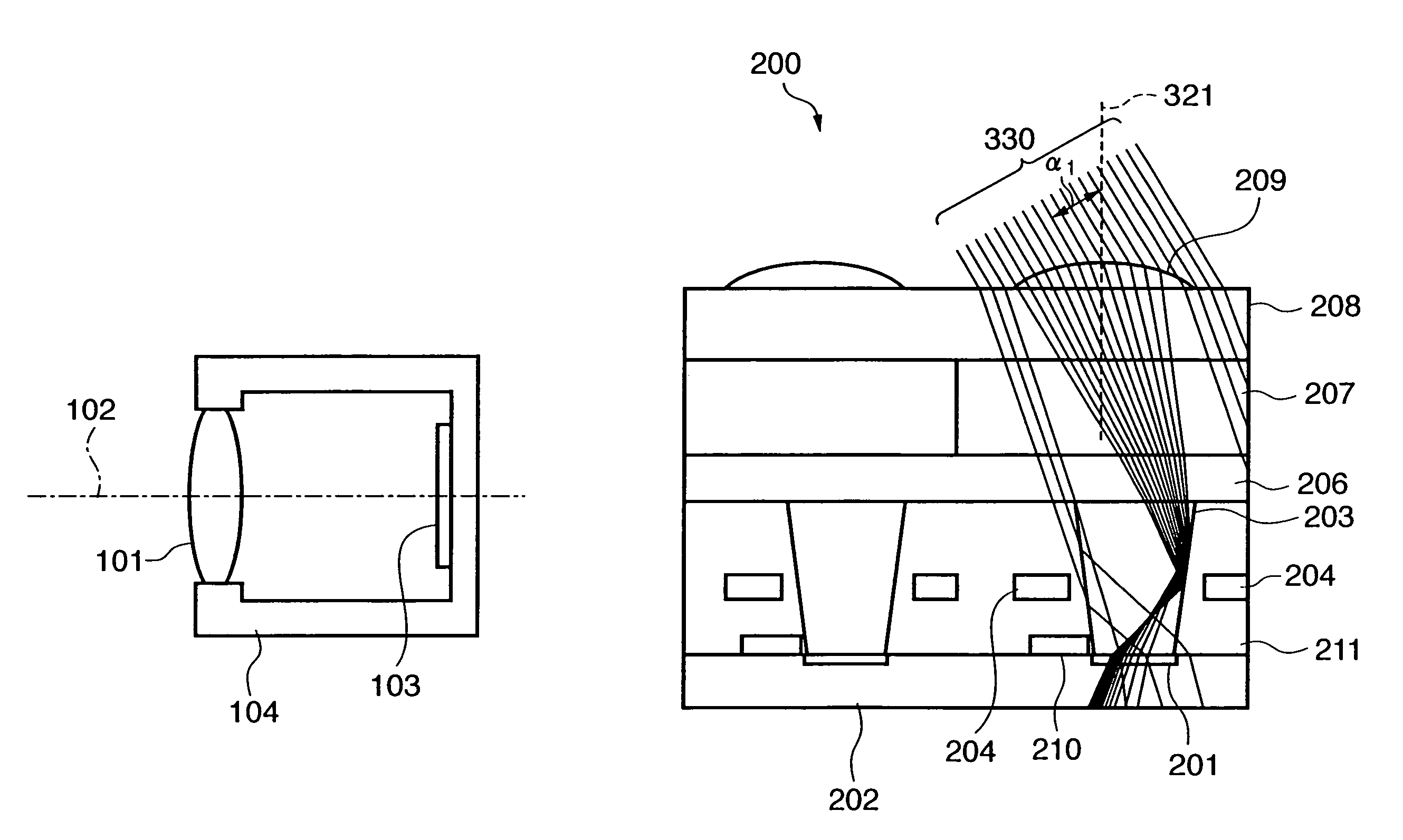
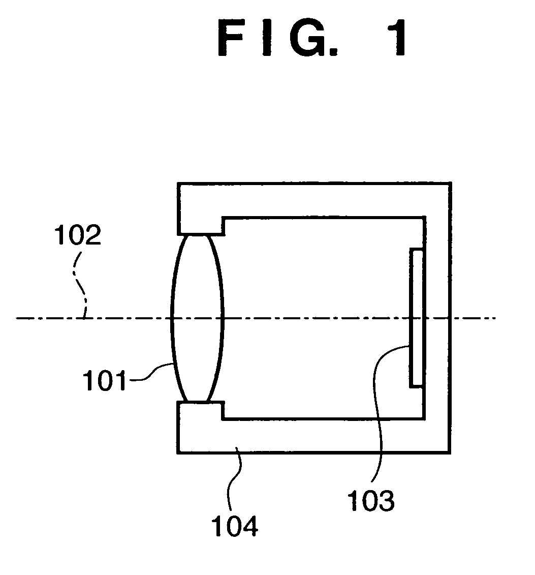
[0097]The relationship between the solid-state image sensing element 200 and pupil redundancy in the first embodiment will be described below.

[0098]As shown in FIG. 2, since the angle the chief ray 107 makes with the optical axis 102 is θ, we have:

[0099]tan⁢⁢θ=HL(1)

Based on this, the relationship among the image height H, pupil distance L, pixel pitch P, height D, refractive index NH of the light guide 203, and refractive index NL of the insulating interlayer 211 is given by:

[0100]H·DL·P<a·NHNL(2)

When the image height H, pupil distance L, pixel pitch P, height D, refractive index NH of the light guide, and refractive index NL of the insulating interlayer are selected to make the coefficient a meet:

0

the effect for the photo-receiving efficiency of the light guides structure can be improved.

[0101]Inequality (2) will be described in detail below.

[0102]FIGS. 7A and 7B are views for explaining the relationship between the refractive index of the light guide 203 and the critic...

second embodiment

[0149]FIG. 14 is a side sectional view showing a schematic structure of a digital color camera as an image sensing device according to the present invention. This camera is a single-plate type digital color camera using an image sensing element such as a CCD, CMOS sensor, or the like, and obtains an image signal indicating a moving or still image by driving the image sensing element continuously or in a one-shot manner. Note that the image sensing element is an area sensor which converts incoming light into charges according to the amount of light, accumulates the charges for respective pixels, and reads out the accumulated charges.

[0150]Referring to FIG. 14, reference numeral 110 denotes a camera body; and 126, a lens device which includes an image sensing lens 125 and is detachable from the camera body 110. Note that FIG. 14 depicts only one lens as the image sensing lens 125. However, the image sensing lens 125 is normally formed by combining a plurality of lenses. The lens devic...

third embodiment

[0220]Furthermore, in the third embodiment, the flattening layer 39 is formed using silicon oxide (SiO2), and the micro convex lens 902 of titanium oxide (TiO2) is formed by etching the upper portion of the flattening layer 39 in a concave shape, forming a titanium oxide (TiO2) layer on top of the etched flattening layer 39, and etching the upper surface of the titanium oxide layer in a convex shape.

[0221]Since the refractive index of silicon oxide (SiO2) that forms the flattening layer 39 is 1.46, and that of titanium oxide (TiO2) that forms the micro convex lens 902 is 2.35, the micro convex lens 902 has a focal length as a convergence system. Therefore, even when there is intervals between the neighboring embedded transparent resin layers 36, a light beam passes through the micro convex lenses 902 which are bedded without any interval, and is efficiently focused on any of embedded transparent resin layers (silicon nitride) 36.

[0222]In this way, the same effect as in the second em...


PUM


Abstract

A solid-state image sensing element has a photoelectric conversion element which converts incoming light into an electrical signal in accordance with an amount of the light, a microlens which is arranged on an incident surface, a light guide which is arranged between the photoelectric conversion element and the microlens, and an insulating interlayer which is arranged around the light guide. The solid-state image sensing element located at a distance (H) satisfies:H·DL·P<a·NHNL⁢⁢for⁢⁢0<a<1where L is the distance from an exit pupil of an image sensing optical system of an image sensing device, which mounts an image sensor formed by two-dimensionally arranging a plurality of the solid-state image sensing elements, H is the distance from a center of the image sensor to a position of the solid-state image sensing element on the image sensor, D is the height from the photoelectric conversion element to an apex of the microlens, P is the spacing between the plurality of solid-state image sensing elements, NH is the refractive index of the light guide, and NL is the refractive index of the insulating interlayer.

Description

FIELD OF THE INVENTION[0001]The present invention relates to an image sensing device having a zoom function and focus adjustment function in an image sensing optical system, a lens-exchangeable image sensing device, a solid-state image sensing element used in the image sensing device and its design support method, and a device.BACKGROUND OF THE INVENTION[0002]In recent years, solid-state image sensing elements mainly used in digital still cameras and the like are roughly classified into a CCD (Charge-Coupled Device) and CMOS (Complementary Metal Oxide Semiconductor) (e.g., see Japanese Patent Laid-Open Nos. 2002-141488 and 2002-083948).[0003]Principal components of the structure of the CCD will be briefly explained first with reference to FIG. 28.[0004]FIG. 28 is a sectional view of one pixel of a CCD 1000. Referring to FIG. 28, reference numeral 1001 denotes a semiconductor substrate formed of, e.g., silicon; 1002, a photoelectric conversion element including a photodiode; 1003, an...

Claims


Application Information

Patent Timeline
Patent Type & Authority Patents(United States)
IPC IPC(8): H01L27/00H01L31/00G02B3/00G02B6/00H01L21/82H01L27/146H01L31/0216H01L31/0232
CPCH01L27/14621H01L27/14625H01L27/14627H01L27/14629H01L31/02162H01L31/0232H01L27/14685H04N2101/00H01L31/02327
Inventor NOTO, GOROSUDA, YASUONAGANO, AKIHIKO
Owner CANON KK
Why Eureka
Try Eureka