Semiconductor light emitting element and light emitting device using this

a technology of light emitting element and semiconductor, which is applied in the direction of discharge tube/lamp details, discharge tube luminescent screen, discharge tube/lamp details, etc., can solve the problem of limited shape of emission spectrum of resultant white-based light, limited number of blue-based, green-based and red-based phosphors exhibiting comparatively high luminous efficiency, etc. problem, to achieve the effect of high luminous efficiency, continuous operation and high luminous flux

Inactive Publication Date: 2007-11-13
PANASONIC CORP
View PDF17 Cites 20 Cited by
  • Summary
  • Abstract
  • Description
  • Claims
  • Application Information

AI Technical Summary

Benefits of technology

[0028]When the above-described phosphor layer is used as a phosphor layer, the semiconductor light emitting device emits light of four colors, that is, blue-based light of a wavelength not less than 400 nm and less than 500 nm, green-based light of a wavelength not less than 500 nm and less than 550 nm, red-based light of a wavelength not less than 600 nm and less than 660 nm, and yellow-based light of a wavelength not less than 55.0 nm and less than 600 nm, so as to emit white-based light through color mixture of these light of four colors. Furthermore, lowering of luminous flux of the white-based light derived from the red-based light, which is good at color purity but is poor at luminosity, is compensated by the yellow-based light with comparatively high luminosity, and therefore, the luminous flux of the white-based light can be improved. Also, since the resultant white-based light attains a spectral distribution with good color balance, an average number of color rendering Ra is also improved.
[0045]All of these blue-based phosphors, green-based phosphors and red-based phosphor are highly efficient phosphors for emitting strong light through excitation by near UV, and therefore, when these phosphors are combined, the phosphor layer can emit white-based light with high luminous intensity.
[0047]A near UV LED having a light emitting layer made of a gallium nitride-based compound semiconductor exhibits high luminous efficiency and can be continuously operated for a long period of time. Therefore, when such a near UV LED is used, a semiconductor light emitting device capable of operating for a long period of time and emitting white-based light with high luminous flux can be obtained.

Problems solved by technology

Therefore, the number of blue-based, green-based and red-based phosphors exhibiting comparatively high luminous efficiency is limited to be small as well as the shape of an emission spectrum of the resultant white-based light is limited.

Method used


Image

  • Semiconductor light emitting element and light emitting device using this
  • Semiconductor light emitting element and light emitting device using this
  • Semiconductor light emitting element and light emitting device using this

Examples


embodiment 1

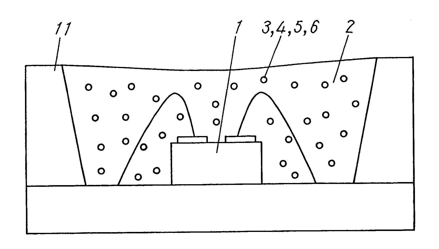
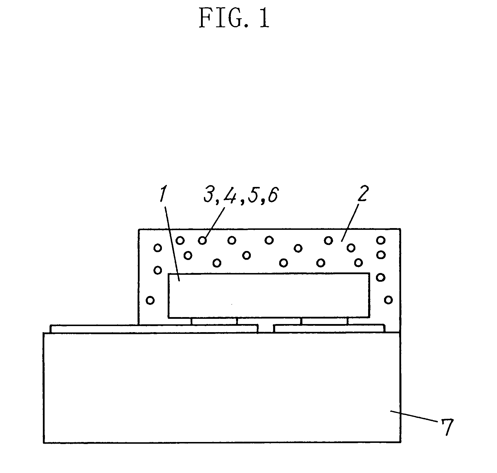
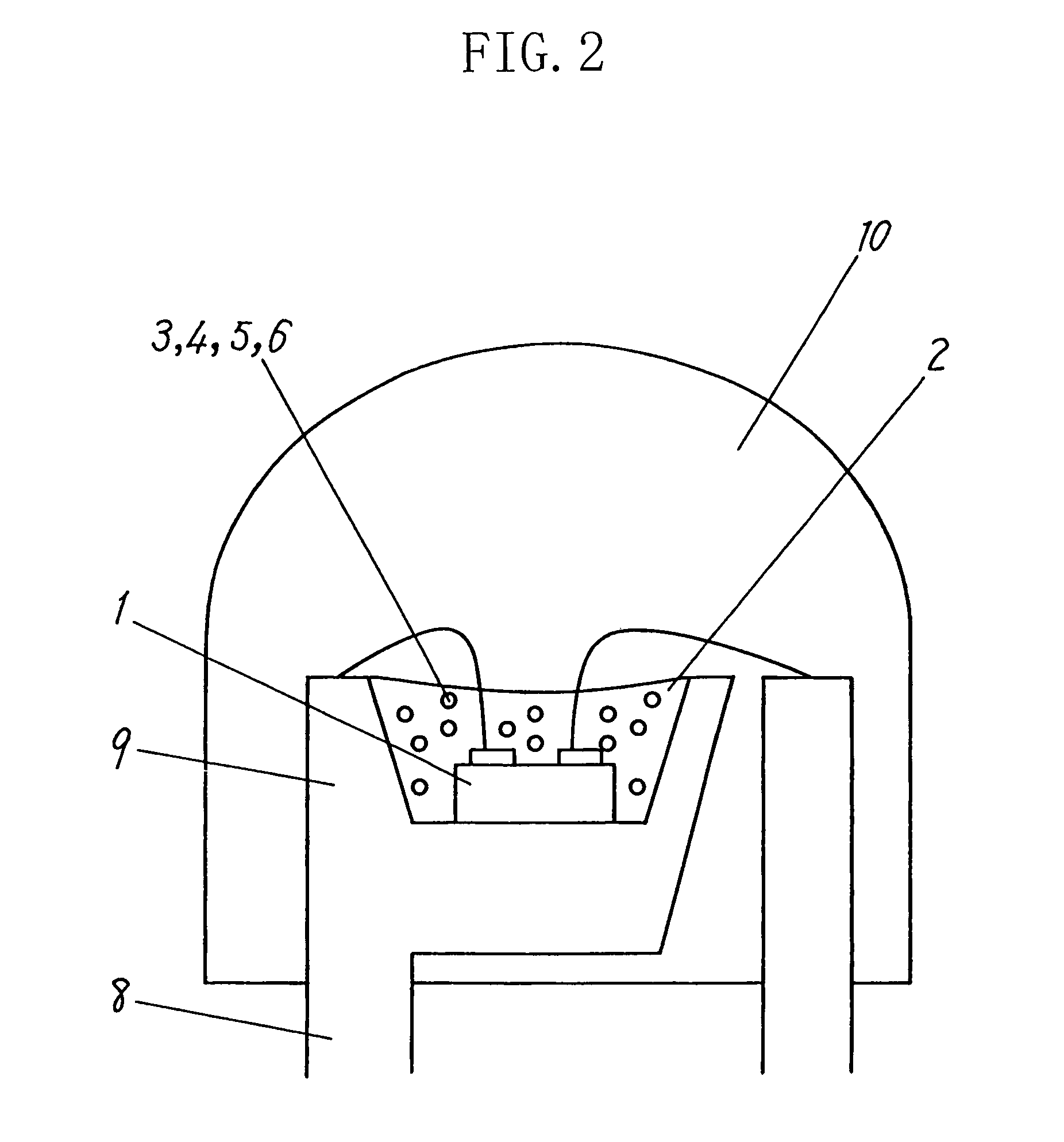
[0072]An embodiment of a semiconductor light emitting device of this invention will now be described with reference to drawings. FIGS. 1 through 3 are longitudinal cross-sectional views of different types of the semiconductor light emitting device.

[0073]Typical examples of the semiconductor light emitting device are the semiconductor light emitting devices shown in FIGS. 1, 2 and 3. FIG. 1 shows a semiconductor light emitting device with a structure in which a flip chip type near UV LED 1 is interface mounted on a sub-mount element 7 and the near UV LED 1 is sealed within a resin package containing phosphor particles including blue-based phosphor particles 3, green-based phosphor particles 4, red-based phosphor particles 5 and yellow-based phosphor particles 6 (hereinafter referred to as BGRY phosphor particles) and working also as a phosphor layer. FIG. 2 shows a semiconductor light emitting device with a structure in which a near UV LED 1 is interface mounted on a cup 9 provided o...

embodiment 2

[0107]An embodiment of a semiconductor light emitting apparatus according to this invention will now be described with reference to drawings. FIGS. 5 through 7 are diagrams of examples of the semiconductor light emitting apparatus of this invention.

[0108]FIG. 5 shows a desk type illumination apparatus using the semiconductor light emitting device of this invention, FIG. 6 shows a display apparatus for image display using the semiconductor light emitting device of this invention, and FIG. 7 shows a display apparatus for numerical indication using the semiconductor light emitting device of this invention.

[0109]In each of FIGS. 5 through 7, a semiconductor light emitting device 12 is the semiconductor light emitting device according to the invention described in Embodiment 1.

[0110]In FIG. 5, a reference numeral 13 denotes a switch for lighting the semiconductor light emitting device 12, and when the switch 13 is turned on, the semiconductor light emitting device 12 is supplied with pow...

example 1

[0121]A semiconductor light emitting device was fabricated by using, as a blue-based phosphor, one represented by a chemical formula, (M21-xEux)(M31-y1Mny1)Al10O17 (wherein M2 is at least one alkali earth metal element selected from the group consisting of Ba, Sr and Ca, M3 is at least one element selected from the group consisting of Mg and Zn, and x and y1 are numerical values satisfying 010O17:Eu2+,Mn2+ aluminate blue phosphor (wherein M2=0.9 Ba+0.1Sr, x=0.1 and y=0.015); as a green-based phosphor, one represented by a chemical formula, (M21-xEux)(M31-y2Mny2)Al10O17 (wherein M2 is at least one alkali earth metal element selected from the group consisting of Ba, Sr and Ca, M3 is at least one element selected from the group consisting of Mg and Zn, and x and y2 are numerical values satisfying 010O17:Eu2+,Mn2+ aluminate green phosphor (wherein x=0.1 and y=0.3); as a red-based phosphor, one represented by a chemical formula, (Ln1-xEux)2O2S (wherein Ln is at least one rare earth eleme...


PUM

PropertyMeasurementUnit
wavelengthaaaaaaaaaa
visible wavelengthaaaaaaaaaa

Abstract

The semiconductor light emitting device is composed of a combination of a near ultraviolet LED and a phosphor layer including a plurality of phosphors for absorbing near ultraviolet emitted by the near ultraviolet LED and for emitting fluorescence having an emission peak in a visible wavelength region, and the phosphor layer includes four kinds of phosphors, that is, a blue-based phosphor, a green-based phosphor, a red-based phosphor and a yellow-based phosphor. Thus, lowering of luminous flux derived from red-based light with low luminosity is compensated by yellow-based light with comparatively high luminosity, and the resultant white-based light can be well color balanced, and hence, a semiconductor light emitting device emitting white-based light with high luminous flux and a large Ra can be obtained.

Description

TECHNICAL FIELD[0001]The present invention relates to a semiconductor light emitting device and a light emitting apparatus for emitting white-based light through a combination of a near ultraviolet light emitting diode (hereinafter referred to as a near UV LED) and a plurality of phosphors.BACKGROUND ART[0002]There conventionally is a known semiconductor light emitting device for emitting white-based light that is composed of a combination of a near UV LED (strictly speaking, a near UV LED chip) having an emission peak in a wavelength region of near UV exceeding 350 nm and not more than 410 nm and a phosphor layer including a plurality of inorganic phosphors each emitting fluorescence having an emission peak in a visible light wavelength range not less than 380 nm and not more than 780 nm. The semiconductor light emitting device using the inorganic phosphors is widely used because it has higher durability than a semiconductor light emitting device using organic phosphors.[0003]It is...

Claims


Application Information

Patent Timeline
Patent Type & Authority Patents(United States)
IPC IPC(8): H01J1/63H01L31/055C09K11/77H01L33/32H01L33/50H05B33/14
CPCC09K11/7734C09K11/7739H05B33/14H01L33/504C09K11/7789H01L33/502H01L2924/181H01L2224/48247H01L2224/48257H01L2224/8592Y02E10/52C09K11/77342H01L2924/00012
Inventor MAEDA, TOSHIHIDEOSHIO, SHOZOIWAMA, KATSUAKIKITAHARA, HIROMI
Owner PANASONIC CORP
Why Eureka
Try Eureka