Manufacturing process of emboss type flexible or rigid printed circuit board

a printed circuit board and flexible technology, applied in the direction of superimposed coating process, resistive material coating, liquid/solution decomposition chemical coating, etc., can solve the problems of high cost, less attractive products, and difficult control and prediction of the price of raw materials by the purchasing department of the company, so as to achieve cost reduction and enhance competitiveness

Inactive Publication Date: 2007-11-20
CHANG ROGER
View PDF6 Cites 11 Cited by
  • Summary
  • Abstract
  • Description
  • Claims
  • Application Information

AI Technical Summary

Benefits of technology

[0006]It is therefore an objective of the present invention to provide a manufacturing process of an emboss type flexible or rigid printed circuit board, which can minimize the disadvantage of high-priced raw materials. The manufacturing process of an embedded type flexible or rigid printed circuit board of the present invention can produce a circuit board with the same effectiveness as the conventional circuit board fabricated by the high-cost surface adhesive technique.
[0012]With the aforesaid steps, the manufacturing process of the embedded type flexible printed circuit board of the present invention does not need use of a conventional carrier, so as to economize on the cost and further enhance competitiveness.

Problems solved by technology

Moreover, when fabricating the circuit board by using the surface adhering technique, excessive cost is inevitable due to high-priced raw materials.
Hence the consumers have to decide between paying more for the state of the art products or choosing lower priced but less attractive products.
Further, it is difficult for purchasing departments of companies to control and even predict the prices of those raw materials, especially when the material purchase orders must be signed long before the products can be manufactured.

Method used


Image

  • Manufacturing process of emboss type flexible or rigid printed circuit board
  • Manufacturing process of emboss type flexible or rigid printed circuit board
  • Manufacturing process of emboss type flexible or rigid printed circuit board

Examples


Embodiment Construction

[0024]According to the aforesaid description of the manufacturing process of the emboss type flexible printed circuit board of the present invention, details are illustrated as follows.

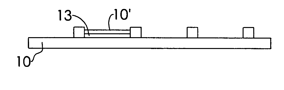
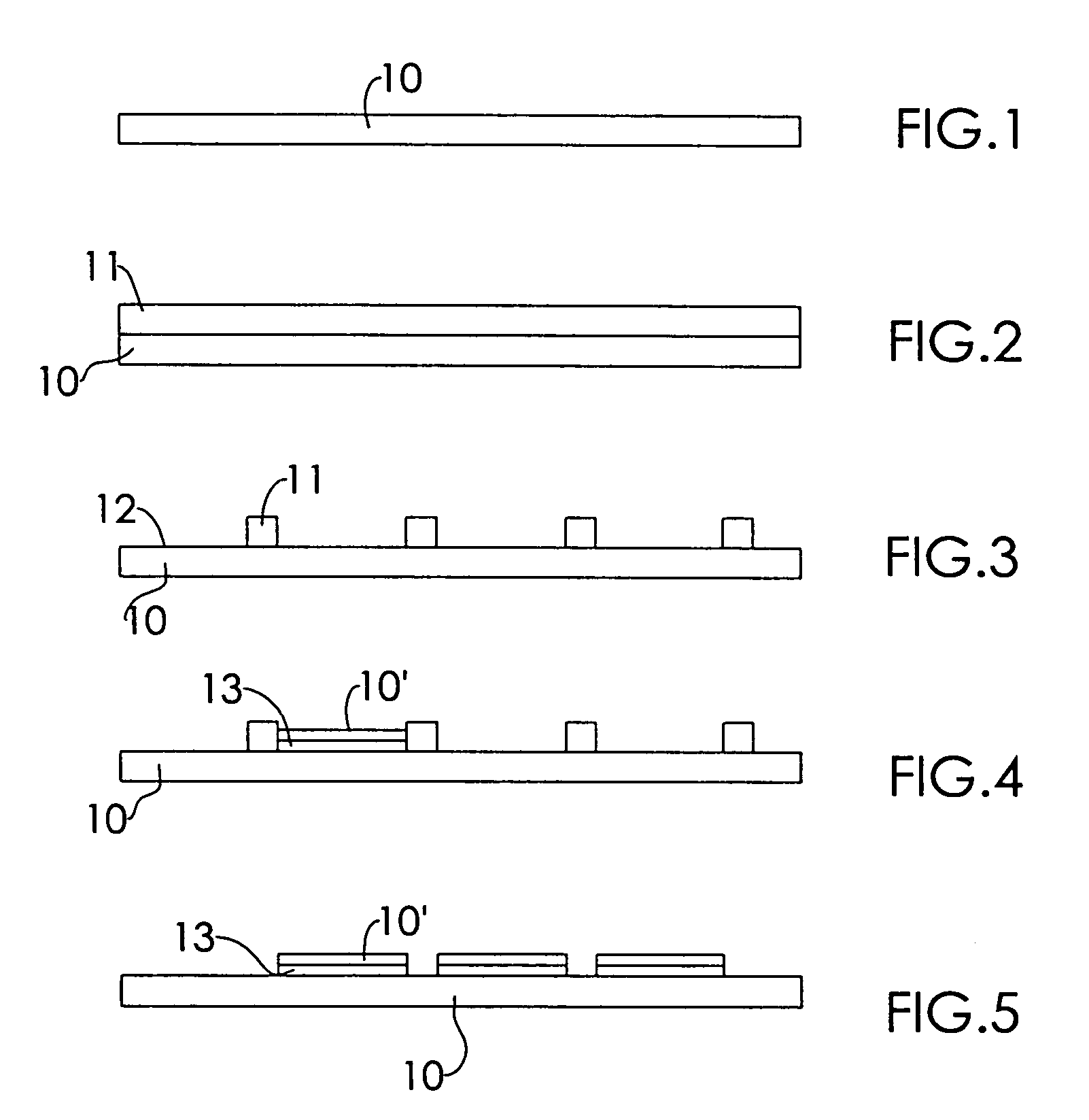
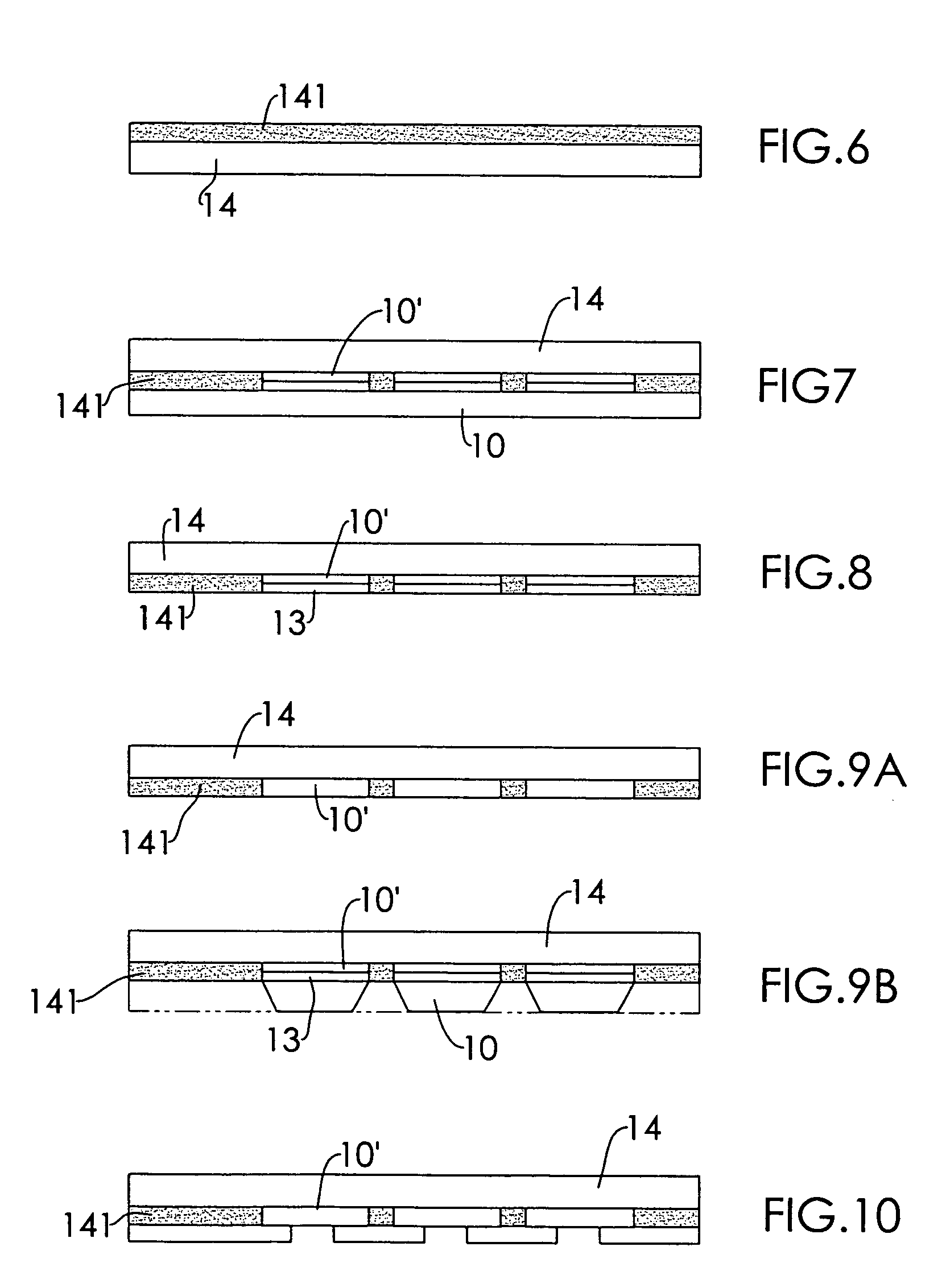
[0025]Referring to FIG. 1 to FIG. 9A, a first step is to prepare a layer of copper foil 10 and the layer of the copper foil 10 is coated with a layer of dry film 11. A circuit pattern 12 is formed on the layer of the copper foil 10 after exposure and development or any conventional method. The circuit pattern 12 is electroplated with an etching stop layer 13 of 3-10 μm. The etching stop layer 13 is electroplated with a layer of copper electroplating 10′. Then the dry film 11 is removed from the layer of the copper foil 10. Next, the copper foil 10 is heated to become soft. An organic surface layer 14 which includes an optional adhesive layer 141 is attached to the copper electroplating 10′ by coating, adhering or compressing. The organic surface layer 14 is then solidified such as by heating or irradi...


PUM

PropertyMeasurementUnit
depthaaaaaaaaaa
flexibleaaaaaaaaaa
structureaaaaaaaaaa

Abstract

A manufacturing process of an emboss type flexible or rigid printed circuit board includes multiple steps. First, a layer of dry film is applied to a layer of copper foil. Then a circuit pattern is formed on the copper foil through photolithography processes. An etching stop layer is electroplated on the circuit pattern. The etching stop layer is then electroplated with copper. The copper foil is softened by a high temperature process after removing the dry film. Then the layer of the copper foil is etched after coating with an organic surface layer and the organic surface layer is solidified.

Description

BACKGROUND OF THE INVENTION[0001]1. Field of the Invention[0002]The invention relates in general to a manufacturing process of an emboss type flexible or rigid printed circuit board, and more particularly to a structure design of an emboss type flexible printed circuit board wherein a circuit is directly formed on a carrier.[0003]2. Description of the Related Art[0004]Semiconductors are manufactured into a huge variety of electronic products. A conventional manufacturing technique for the semiconductors is to fabricate multiple pre-manufactured grain-shaped chips into semiconductor elements having external contacts or pins. Then the contacts or the pins of the semiconductor elements are soldered to be coupled with a circuit on a circuit board, so as to manufacture the electronic products with predetermined functions.[0005]However, as the overwhelming trend in electronic products is towards developing portable and compact devices, a surface adhering technique is applied to secure the...

Claims


Application Information

Patent Timeline
Patent Type & Authority Patents(United States)
IPC IPC(8): H01B13/00
CPCH05K3/205H05K1/0393H05K3/064H05K3/386H05K2203/1105H05K2201/0355H05K2201/0367H05K2203/0384H05K3/4007
Inventor CHANG, ROGER
Owner CHANG ROGER
Why Eureka
Try Eureka