Image forming apparatus

a technology of forming apparatus and el element, which is applied in the direction of instruments, discharge tubes luminescnet screens, recording apparatus, etc., can solve the problems of accelerating deterioration of el elements, affecting the el element deterioration, so as to reduce the deterioration of elements and stable light

Active Publication Date: 2007-11-20
SEIKO EPSON CORP
View PDF16 Cites 13 Cited by
  • Summary
  • Abstract
  • Description
  • Claims
  • Application Information

AI Technical Summary

Benefits of technology

[0008]The present invention was made in view of the aforementioned problems of conventional techniques and the object of the present invention is to provide an image forming apparatus which is structured to ensure stable amount of light when organic EL elements are used as light emitting elements in a line head and to reduce the deterioration of the elements.

Problems solved by technology

However, according to this control method, direct current bias is applied to inorganic EL elements even during non-printing.
Further, organic compound as a component of the organic EL element has a characteristic of being susceptible to water.
This example has a problem that the deterioration of the EL elements is accelerated because the organic EL elements are actually lighted.
That is, there is a problem that the amount of emitted light varies according to the variation in temperature of the organic EL elements.
Because the deterioration of the organic EL element is accelerated by the light emission, there is also a problem that differences in degree of deterioration among the elements lead to variation in light emission.
Application of voltage exceeding the light emitting voltage shortens the lives of the organic EL elements.
There is a problem that structure of the line head is complex because a temperature detecting means is provided and the control circuit is complex because a temperature control circuit is added.

Method used


Image

  • Image forming apparatus
  • Image forming apparatus
  • Image forming apparatus

Examples


Embodiment Construction

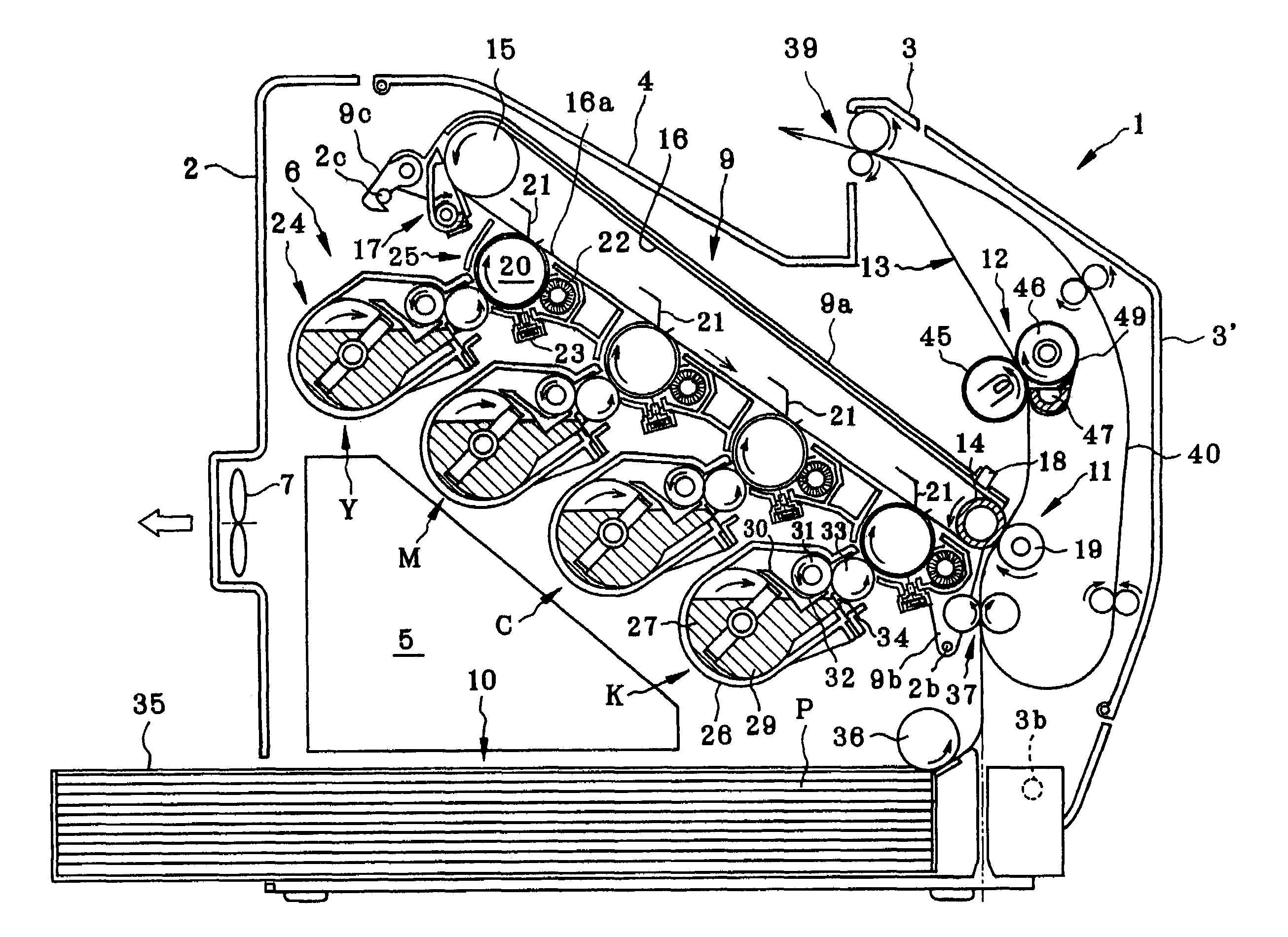
[0066]Hereinafter, an embodiment of an image forming apparatus according to the present invention will be described with reference to the attached drawings. FIG. 1 is a schematic sectional view showing the entire structure of the embodiment of the image forming apparatus to which the present invention is adopted. This embodiment is of a type employing an intermediate transfer belt as a transfer belt. In FIG. 1, the image forming apparatus 1 of this embodiment comprises a housing body 2, a first door member 3 which is disposed on the front of the housing body 2 such that the first door member is openable and closable, and a second door member (also functioning as an outfeed tray) 4 which is disposed on the top of the housing body 2 such that the second door member is openable and closable. The first door member 3 is provided with a lid 3′ which is disposed such that the lid 3′ is openable and closable relative to the front of the housing body 2. The lid 3′ can be opened and closed in...


PUM


Abstract

Image data is inputted from a data processing means 123 into storage means 124 so that light emitting elements of one line 128a of a light-emitting element (yellow) line head 128 are activated to expose pixels on an image carrier according to an output signal form a shift resistor 124a. The image carrier is moved in the direction of arrow X in such a manner that the pixels reach a position corresponding to the light emitting elements in a next line 128b. At this point of time, the image data are transmitted to a shift resistor 124b and then outputted to the line 128b so as to expose the pixels again. The image data are transmitted among the shift resistors sequentially by moving the image carrier, thereby sequentially repeatedly expose the same pixels.

Description

BACKGROUND OF THE INVENTION[0001]The present invention relates to an image forming apparatus which is structured to ensure stable amount of light when organic EL elements are used as light emitting elements in a line head and to reduce the deterioration of the elements.[0002]In conventional image forming apparatus in which a latent image is written on an image carrier, it is common practice to employ an LED (light emitting diode) array as writing means. Line head in which light elements such as LEDs are aligned in plural lines has been developed. For example, Japanese Patent No. 2534364 discloses such a line head in which EL elements are used to form arrays. As the application of driving pulse to the EL elements is finished, the afterglow is reduced. Accordingly, as the driving pulse is applied after non-emission for a long time, the time required to reach a predetermined light intensity becomes longer and, in addition, the amount of emitted light becomes smaller. For this, in Japan...

Claims


Application Information

Patent Timeline
Patent Type & Authority Patents(United States)
IPC IPC(8): H01J1/62B41J2/435B41J2/447B41J2/47G03G15/01G03G15/04
CPCB41J2/447G03G15/04072G03G2215/0412
Inventor KITAZAWA, ATSUNORINOMURA, YUJIROTSUJINO, KIYOSHI
Owner SEIKO EPSON CORP
Why Eureka
Try Eureka