

Organic light emitting diode display with insulating film which contains SiO
a light-emitting diode and organic technology, applied in the field of active matrix type organic light-emitting diode display, can solve the problems of poor inability to fundamentally improve the emission coupling efficiency, and unclear whether the thin film transistor circuit can withstand high pressure or not, so as to reduce the coupling-out efficiency of emission from the organic electroluminescence layer to the outside, the effect of reducing the correlation between the film density and the light scatter
- Summary
- Abstract
- Description
- Claims
- Application Information
AI Technical Summary
Benefits of technology
Problems solved by technology
Method used
Image

Examples
example 1
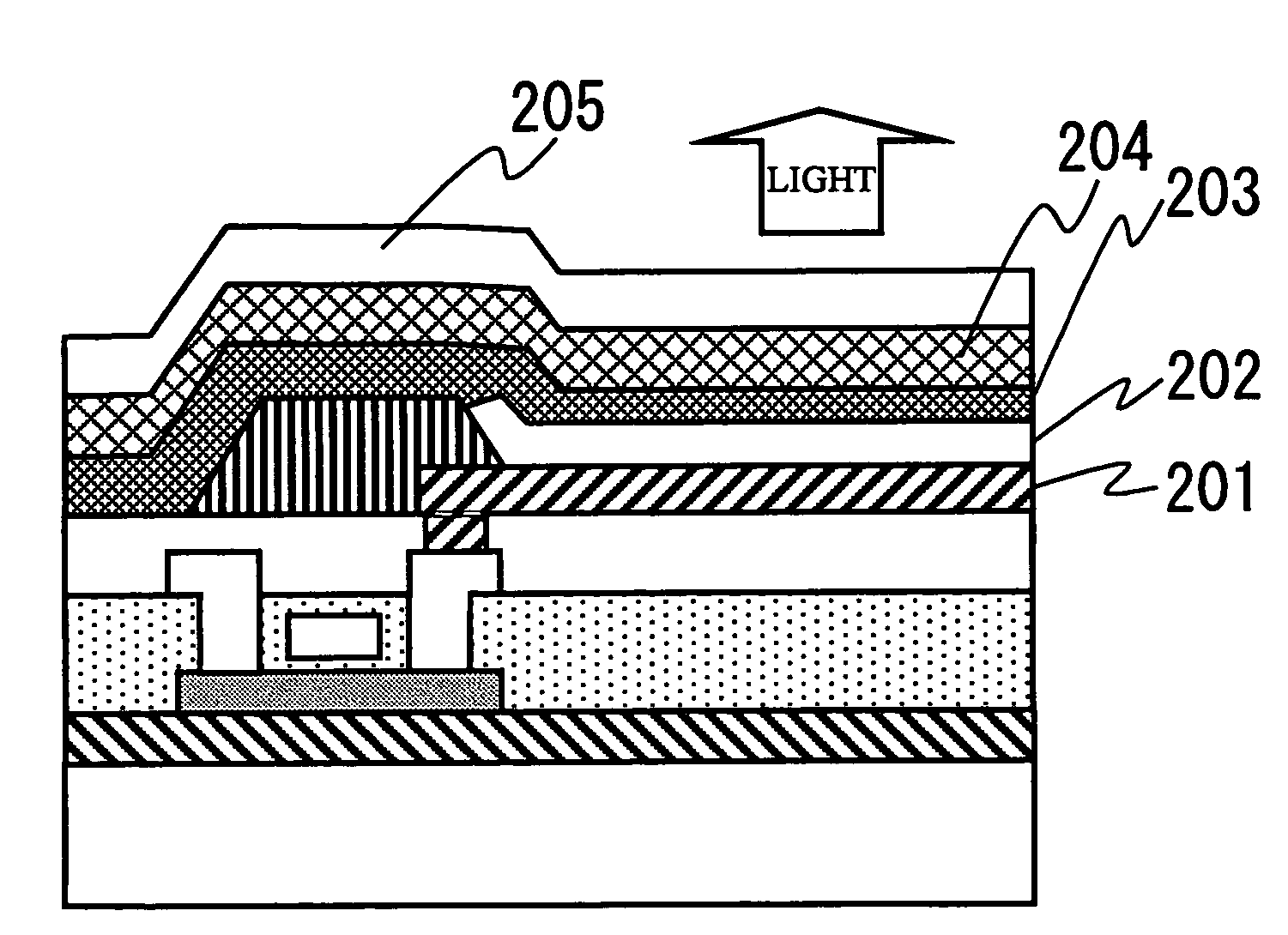
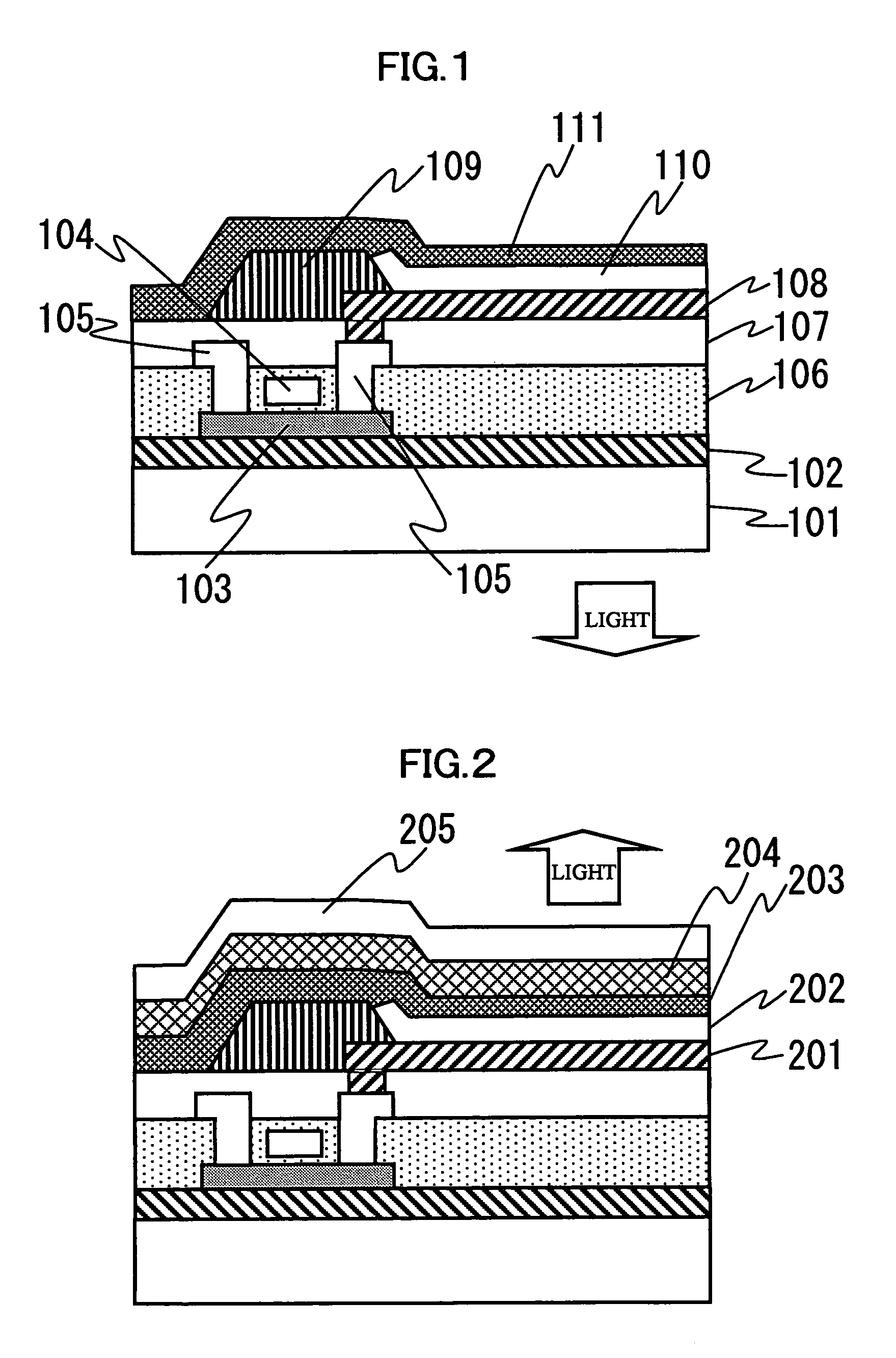
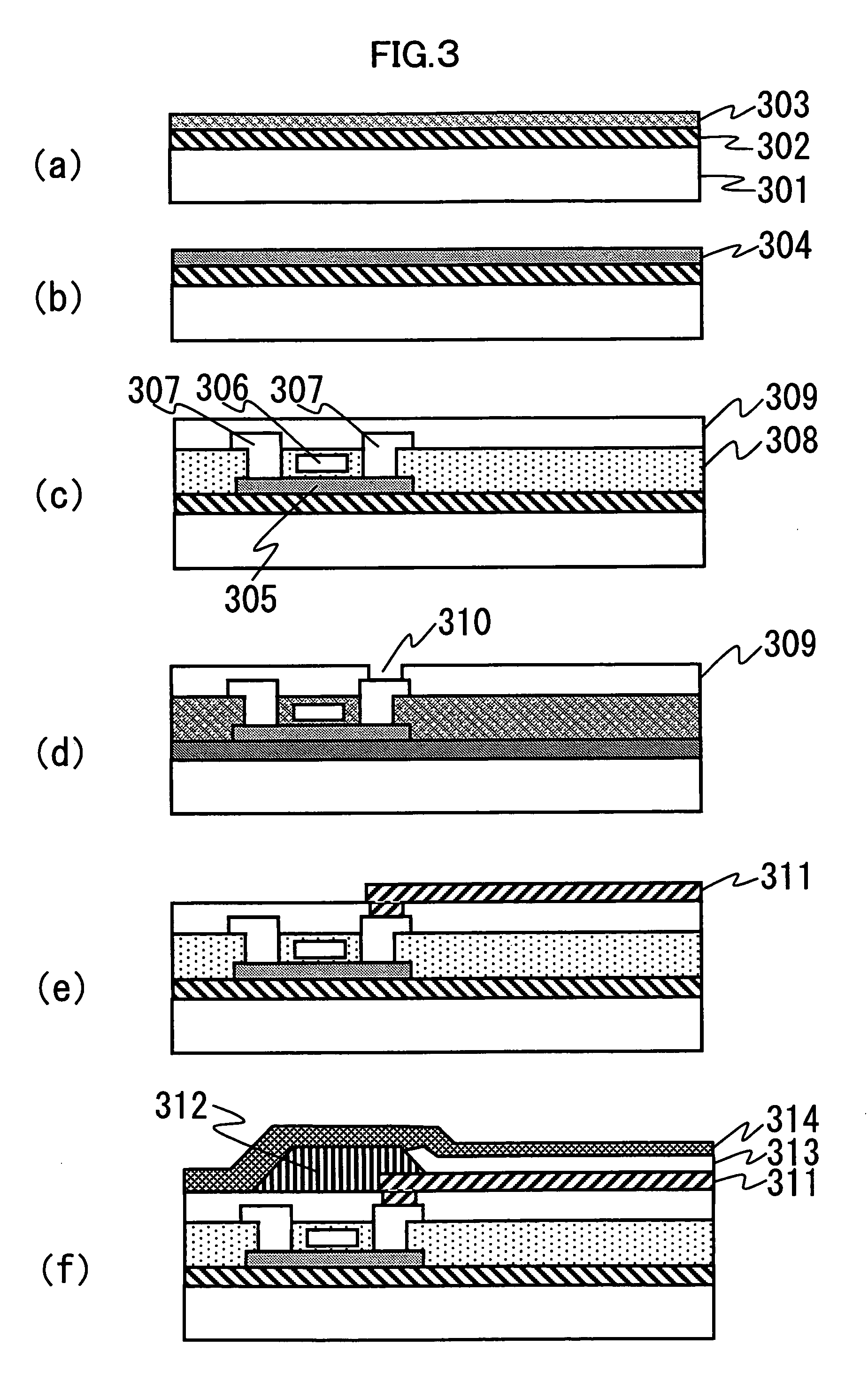
[0096]An OLED display whose sectional view is shown in FIG. 1 was manufactured in the following conditions. In FIG. 1, the undercoat insulator 102 was formed out of an SiN film 100 nm thick and an SiO film 50 nm thick thereon by a CVD method so as to have a total thickness of 150 nm. The interlayer insulator 106 was formed out of an SiO film 400 nm thick by use of a CVD method. The pixel separating insulator 109 was formed out of an SiN film 150 nm thick by use of a CVD method.
[0097]A methyl isobutyl ketone application solution containing a hydrogen silsesquioxane compound as its chief component was applied to a substrate as the insulator 107 contacting with the anode transparent electrode 108. After that, by use of a hot plate heating system, the substrate was heated at 100° C. for 10 minutes, at 150° C. for 10 minutes, at 230° C. for 10 minutes and at 350° C. for 10 minutes in an inert atmosphere such as a nitrogen atmosphere. Thus, Si—O—Si bonds were formed like a ladder structur...
example 2
[0116]A methyl isobutyl ketone application solution containing a methyl silsesquioxane compound as its chief component was applied to a substrate as the insulator 107 contacting with the anode transparent electrode 108. After that, by use of a hot plate heating system, the substrate was heated at 100° C. for 10 minutes, at 150° C. for 10 minutes, at 230° C. for 10 minutes and at 350° C. for 10 minutes in an inert atmosphere such as a nitrogen atmosphere. Thus, Si—O—Si bonds were formed like a ladder structure, and finally formed into a porous insulating film containing SiO as its chief component.
[0117]On this occasion, the porous insulating film had the following properties.
Film Thickness: 230 nm, Density: 1.25 g / cm3, Refractive Index: 1.30, Film Hardness: 4.6 GPa, Film Elasticity: 3.2 GPa, Average Nano Pore Diameter in Film: 2.3 nm
[0118]An OLED display was manufactured in the same conditions as in Example 1, except the aforementioned film. The OLED display was turned on in the same...
example 3
[0121]A methyl isobutyl ketone application solution containing a hydrogen silsesquioxane compound different from that in Example 1 as its chief component was applied to a substrate as the insulator 107 contacting with the anode transparent electrode 108. After that, by use of a hot plate heating system, the substrate was heated at 100° C. for 10 minutes, at 150° C. for 10 minutes, at 230° C. for 10 minutes and at 350° C. for 10 minutes in an inert atmosphere such as a nitrogen atmosphere. Thus, Si—O—Si bonds were formed like a ladder structure, and finally formed into a porous insulating film containing SiO as its chief component.
[0122]On this occasion, the porous insulating film had the following properties.
Film Thickness: 230 nm, Density: 1.42 g / cm3, Refractive Index: 1.33, Film Hardness: 0.53 GPa, Film Elasticity: 6.7 GPa, Average Nano Pore Diameter in Film: 1.1 nm, Maximum Nano Pore Diameter in Film: 0.64 nm
[0123]An OLED display was manufactured in the same conditions as in Exam...
PUM
| Property | Measurement | Unit |
|---|---|---|
| temperature | aaaaa | aaaaa |
| density | aaaaa | aaaaa |
| refractive index | aaaaa | aaaaa |
Abstract
Description
Claims
Application Information