Solid-state imaging device, method for manufacturing solid-state imaging device, and electronic apparatus

Inactive Publication Date: 2010-04-01
SONY CORP
View PDF19 Cites 42 Cited by
  • Summary
  • Abstract
  • Description
  • Claims
  • Application Information

AI Technical Summary

Benefits of technology

[0035]The diffuse reflection and the interfacial reflection can be suppressed by the solid-state imaging device according to an embodiment of the present invention. Therefore, the sensitivity is improved and an occurrence of image variation can be suppressed.
[0036]A solid-state imaging device, in which the sensitivity is improved and an occurrence of image variation can be suppressed, can be produced by

Problems solved by technology

Regarding a solid-state imaging device, in particular a CCD solid-state imaging device, it has become difficult to maintain the sensitivity, the smear characteristic, and other optical characteristics along with cell size reduction of the pixel.
Conversely, as the depositi

Method used


Image

  • Solid-state imaging device, method for manufacturing solid-state imaging device, and electronic apparatus
  • Solid-state imaging device, method for manufacturing solid-state imaging device, and electronic apparatus
  • Solid-state imaging device, method for manufacturing solid-state imaging device, and electronic apparatus

Examples


first embodiment

1. First Embodiment

Configuration Example of Solid-State Imaging Device

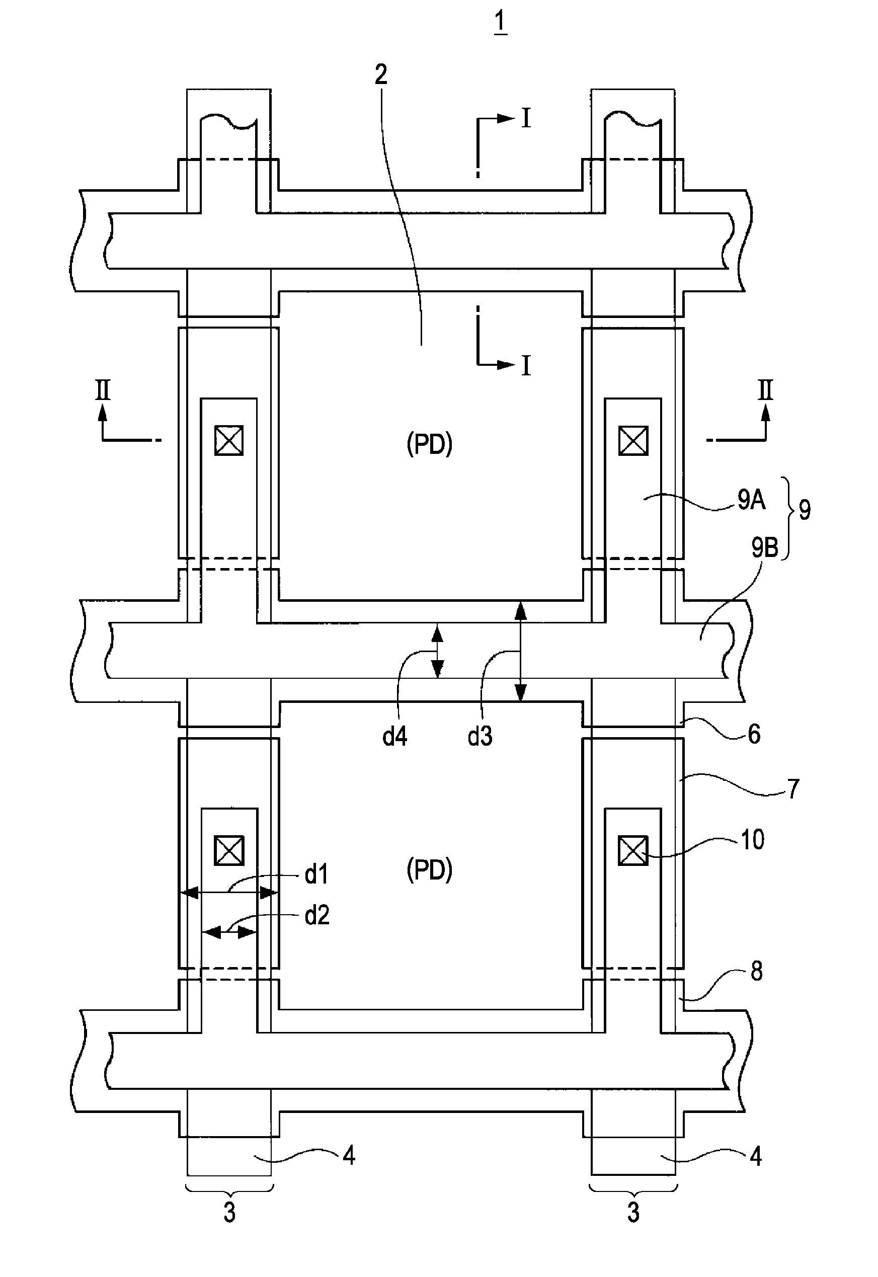
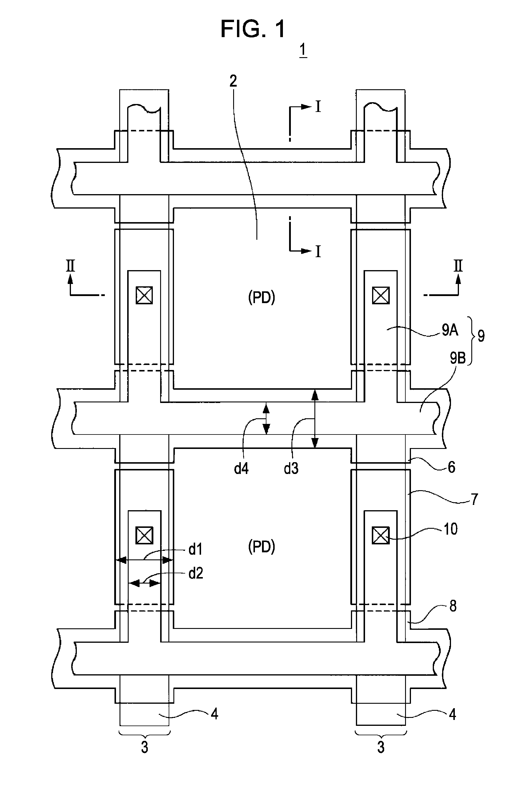
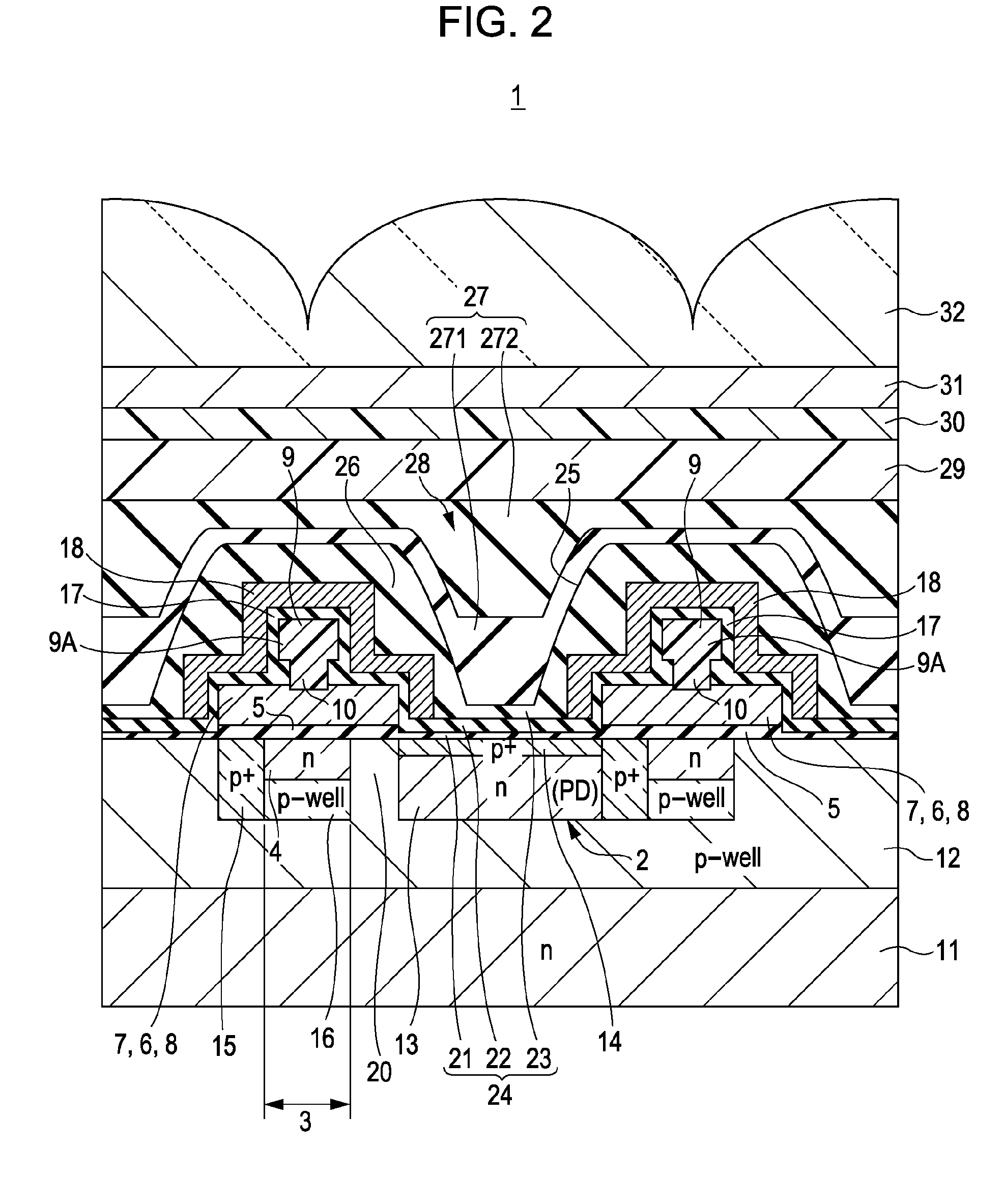
[0078]FIG. 1 and FIG. 2 show a first embodiment in which a solid-state imaging device according to an embodiment of the present invention is applied to a CCD solid-state imaging device. FIG. 1 is a plan view of a key portion of an imaging region of the CCD solid-state imaging device according to a first embodiment of the present invention. FIG. 2 is a sectional view of a section taken along a line II-II shown in FIG. 1.

[0079]As shown in FIG. 1, a solid-state imaging device 1 according to the first embodiment has an imaging region including light-receiving portions 2, which are in the shape of, for example, a square or a rectangle, while a square is employed in the present example, and which are arranged two-dimensionally, and vertical transfer resister portions 3, which have a CCD structure and which are disposed in accordance with the individual lines of the light-receiving portions 2. The light-receiving portion...

second embodiment

2. Second Embodiment

Configuration Example of Solid-State Imaging Device

[0131]FIG. 14 shows a second embodiment in which a solid-state imaging device according to an embodiment of the present invention is applied to a CCD solid-state imaging device. FIG. 14 is a sectional view of a key portion of an imaging region of the CCD solid-state imaging device. In a solid-state imaging device 51 according to the present embodiment, a waveguide 28 including a clad layer 26 and a core layer 27 is disposed on a photodiode (PD) serving as a light-receiving portion 2, the core layer 27 including a first film 271 exhibiting good embeddability and having a relatively low refractive index and a second film 272 having a high refractive index. This waveguide 28 is the same waveguide as described in the first embodiment.

[0132]In the configuration of the present embodiment, in particular, a low-refractive index silicon oxide film 23 is not disposed on an antireflection film 22 and the first film 271 of t...

third embodiment

3. Third Embodiment

Configuration Example of Solid-State Imaging Device

[0139]FIG. 17 shows a third embodiment in which a solid-state imaging device according to an embodiment of the present invention is applied to a CCD solid-state imaging device. FIG. 17 is a sectional view of a key portion of an imaging region of the CCD solid-state imaging device. In a solid-state imaging device 53 according to the present embodiment, an intra-layer lens 54 is further disposed on the above-described waveguide 28. That is, regarding the solid-state imaging device 53 according to the present embodiment, a waveguide 28 is disposed on a photodiode (PD) serving as a light-receiving portion 2 while including a clad layer 26 and a core layer 27 embedded in the trench portion of the clad layer 26. The core layer 27 includes a first film 271 and a second film 272. The first film 271 serving as the lower layer constituting the core layer exhibits good embeddability and has a relatively low refractive index ...


PUM


Abstract

A solid-state imaging device includes a light-receiving portion, which serves as a pixel, and a waveguide, which is disposed at a location in accordance with the light-receiving portion and which includes a clad layer and a core layer embedded having a refractive index distribution in the wave-guiding direction.

Description

BACKGROUND OF THE INVENTION[0001]1. Field of the Invention[0002]The present invention relates to a solid-state imaging device, a method for manufacturing the solid-state imaging device, and an electronic apparatus including the solid-state imaging device.[0003]2. Description of the Related Art[0004]Solid-state imaging devices are roughly classified into charge transfer type solid-state imaging devices typified by a CCD image sensor and amplification type solid-state imaging devices typified by a CMOS image sensor. In this regard, “CCD” is the abbreviated name for a charge coupled device, and “CMOS” is the abbreviated name for a complementary metal oxide semiconductor.[0005]A CCD solid-state imaging device includes an imaging region including a plurality of light-receiving portions arranged two-dimensionally, that is, photodiodes serving as photoelectric conversion elements, and vertical transfer resister portions which are arranged in accordance with the individual photodiode lines ...

Claims


Application Information

Patent Timeline
IPC IPC(8): H01L31/0232H01L27/14H01L27/148H04N5/335H04N5/359H04N5/369H04N5/372H04N5/374
CPCH01L27/14603H01L27/14629H01L27/14685H01L27/146
Inventor WANO, HIROMITANIKUNI, TAKAMASAYOSHIDA, SHINICHI
Owner SONY CORP
Why Eureka
Try Eureka