Non-volatile semiconductor memory device adapted to store a multi-valued in a single memory cell

a non-volatile, memory cell technology, applied in static storage, digital storage, instruments, etc., can solve the problems of reducing the distance between the floating gate, reducing the performance of controlling the threshold voltage, and producing problems, so as to and reduce the rate of changing the write state

Inactive Publication Date: 2007-11-27
KIOXIA CORP
View PDF14 Cites 21 Cited by
  • Summary
  • Abstract
  • Description
  • Claims
  • Application Information

AI Technical Summary

Benefits of technology

[0017]In an aspect of the present invention, there is provided a non-volatile semiconductor memory device comprises: an electrically data rewritable non-volatile semiconductor memory cell; and a write circuit configured to write data to the memory cell by supplying a write voltage and a write control voltage to the memory cell to change the write state of the memory cell, changing the supply of the write control voltage to reduce the rate of changing the write state, further changing the supply of the write control voltage to control the reduced rate of changing the write state and terminating the write operation to the memory cell while the rate of changing the write state is reduced.

Problems solved by technology

This means that the gaps separating memory cells are made smaller and smaller to consequently give rise to various problems from the viewpoint of multi-valued flash memories.
For instance, the distance separating floating gates is reduced to produce problems as pointed out below as a result of micronization.
Additionally, the performance of controlling the threshold voltage is not necessarily satisfactory.
Therefore, so far, any attempt at securing a write out margin and raising the reliability of a memory device is accompanied by the problem of an increased write time.

Method used


Image

  • Non-volatile semiconductor memory device adapted to store a multi-valued in a single memory cell
  • Non-volatile semiconductor memory device adapted to store a multi-valued in a single memory cell
  • Non-volatile semiconductor memory device adapted to store a multi-valued in a single memory cell

Examples


first embodiment

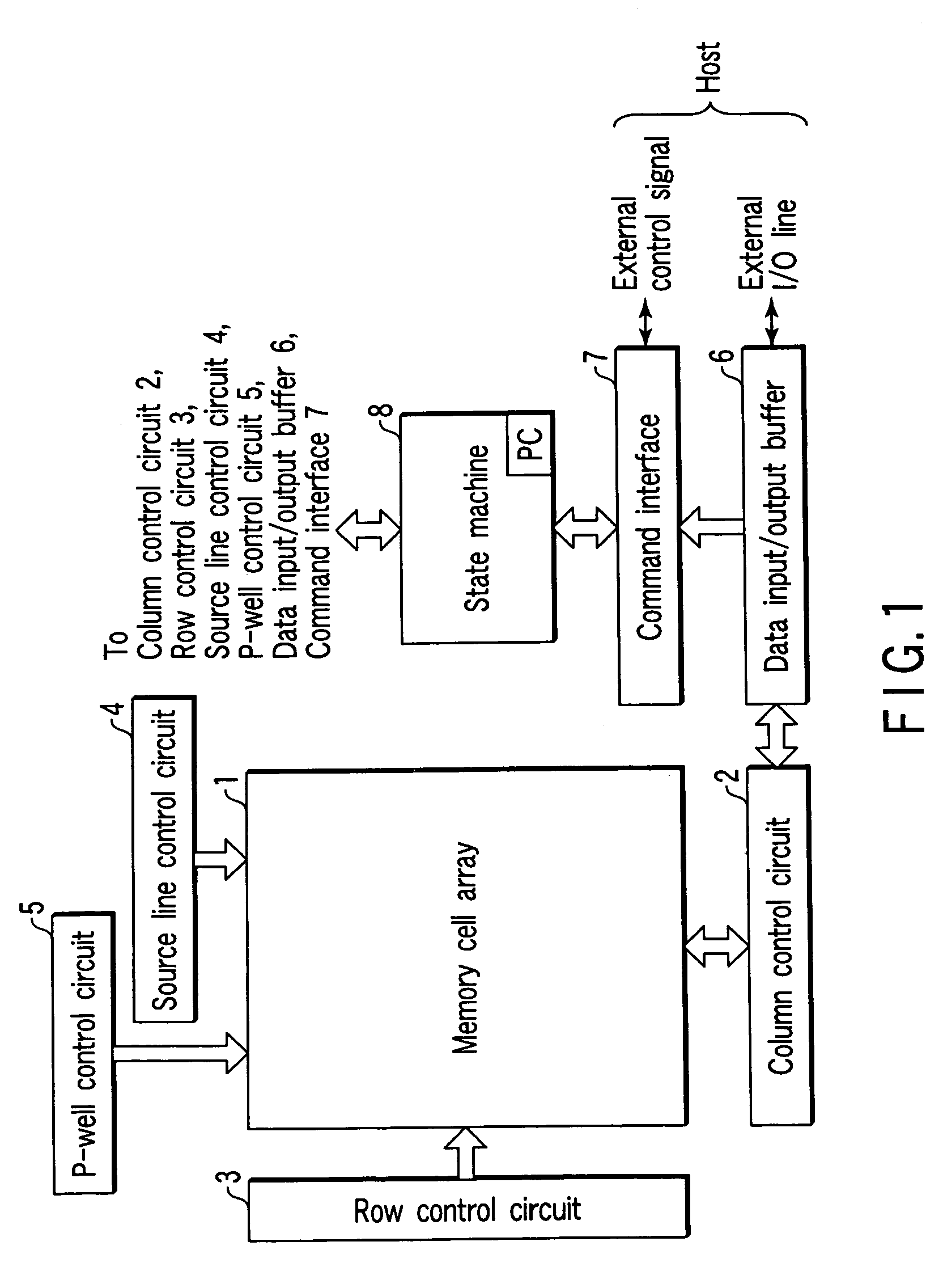
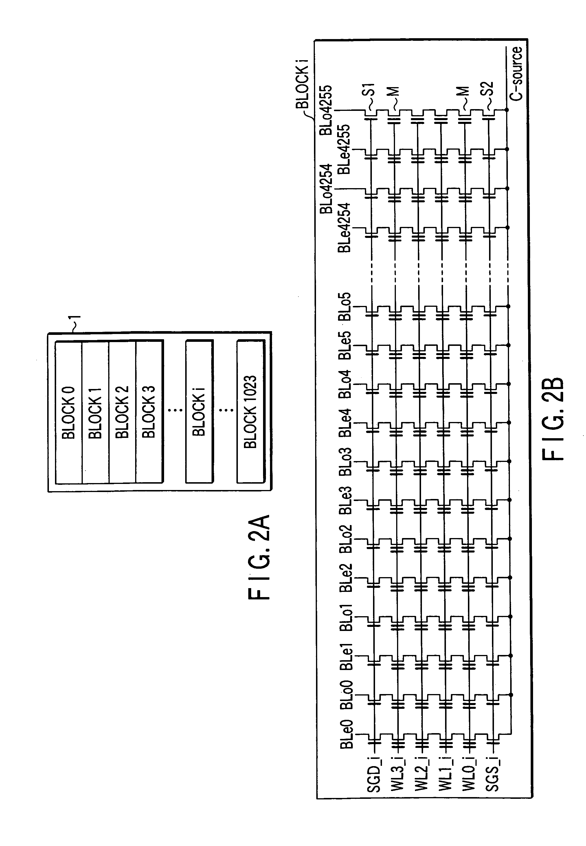
[0049]FIG. 1 is a schematic block diagram of multi-value flash memory, illustrating its overall configuration. Referring to FIG. 1, a plurality of flash memory cells, a plurality of bit lines and a plurality of word lines are arranged in the memory cell array 1. The flash memory cells are arranged in the form of a matrix.

[0050]A column control circuit 2 and a row control circuit 3 are arranged adjacently relative to the memory cell array 1. The column control circuit 2 controls the bit lines in the memory cell array 1 for erasing data from, writing data into and reading data from memory cells.

[0051]The row control circuit 3 is used for selecting a word line in the memory cell array 1 and supplying a voltage necessary for erasing, writing and reading data.

[0052]Additionally, a source line control circuit 4 for controlling source lines of the memory cell array 1 and a P-well control circuit 5 for controlling a voltage of the p-type wells for forming the memory cell array 1 are also ar...

second embodiment

[0136]Now, the present invention will be described below.

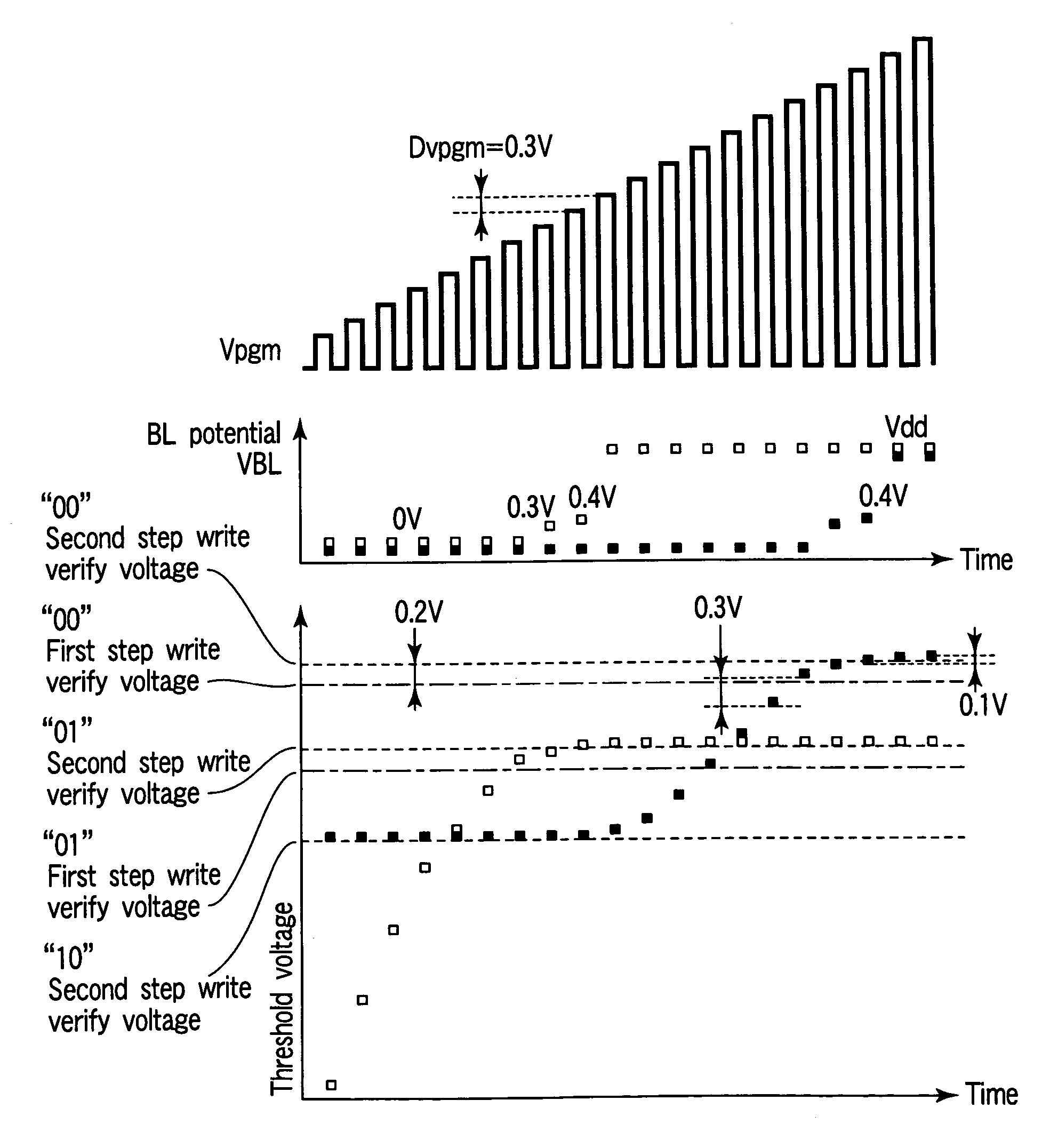
[0137]FIG. 14 is a graph illustrating the signal waveforms in a write step of the first embodiment of flash memory. The voltage of bit line BLe is made equal to 0.3V immediately after a write operation for the second step write operation. In a write step of the first embodiment, the voltage of bit line BLe, which is the write control voltage, is raised stepwise from 0.3V by 0.1V at a time for a write operation while a predetermined write voltage (18.0V in the illustrated example) is being applied to word line WL (WL2).

[0138]To the contrary, in the second embodiment, the voltage (VBL) of the bit line BLe, which is the write control voltage, is not raised to 0.3V immediately after the start of the second step write operation but, as shown in FIG. 15, the voltage of the bit line BLe, which is the write control voltage, is made equal to 0V for a predetermined period of time (Twr in FIG. 15) out of the time period during which the ...


PUM


Abstract

A non-volatile semiconductor memory device includes a non-volatile memory cell and a write circuit that is adapted to write data to the memory cell by supplying a write voltage and a write control voltage to the memory cell to change the write state of the memory cell, changing the supply of the write control voltage to reduce the rate of changing the write state, further changing the supply of the write control voltage to control the reduced rate of changing the write state and terminating the write operation to the memory cell while the rate of changing the write state is reduced.

Description

CROSS-REFERENCE TO RELATED APPLICATIONS[0001]This application is a Divisional of U.S. application Ser. No. 10 / 051,372 filed on Jan. 22, 2002, now U.S. Pat. No. 6,643,188 hereby incorporated by reference as to its entirety. This application is based upon and claims the benefit of priority from the prior Japanese Patent Application No. 2003-410237, filed Dec. 9, 2003, the entire contents of which are incorporated herein, by reference.BACKGROUND OF THE INVENTION[0002]1. Field of the Invention[0003]This invention relates to an electrically data rewritable non-volatile semiconductor memory device. More particularly, it relates to a multi-value flash memory adapted to store a multi-valued data in a memory cell.[0004]2. Description of the Related Art[0005]In a flash memory, the accumulated electric charge of the floating gate of a memory cell transistor is changed as the stored data is erased and a new data is written there. Then, as a result, the threshold voltage is changed to store the ...

Claims


Application Information

Patent Timeline
Patent Type & Authority Patents(United States)
IPC IPC(8): G11C11/00G11C11/56
CPCG11C16/0483G11C11/5628
Inventor TANAKA, TOMOHARU
Owner KIOXIA CORP
Why Eureka
Try Eureka