
Sense amplifier circuitry and architecture to write data into and/or read from memory cells

a memory cell and logic circuit technology, applied in semiconductor devices, digital storage, instruments, etc., can solve the problems of reducing the margin of read operation, adding complexity and latency to the read operation, and writing back operations

Active Publication Date: 2007-11-27
MICRON TECH INC
View PDF219 Cites 158 Cited by
  • Summary
  • Abstract
  • Description
  • Claims
  • Application Information

AI Technical Summary

Problems solved by technology

The bit line selection circuitry often adds complexity and latency to the read as well as write back operations.
In addition, the bit line selection circuitry may introduce unwanted capacitance and inductance which may reduce the margin of the read operation.

Method used


Image

  • Sense amplifier circuitry and architecture to write data into and/or read from memory cells
  • Sense amplifier circuitry and architecture to write data into and/or read from memory cells
  • Sense amplifier circuitry and architecture to write data into and/or read from memory cells

Examples


Embodiment Construction

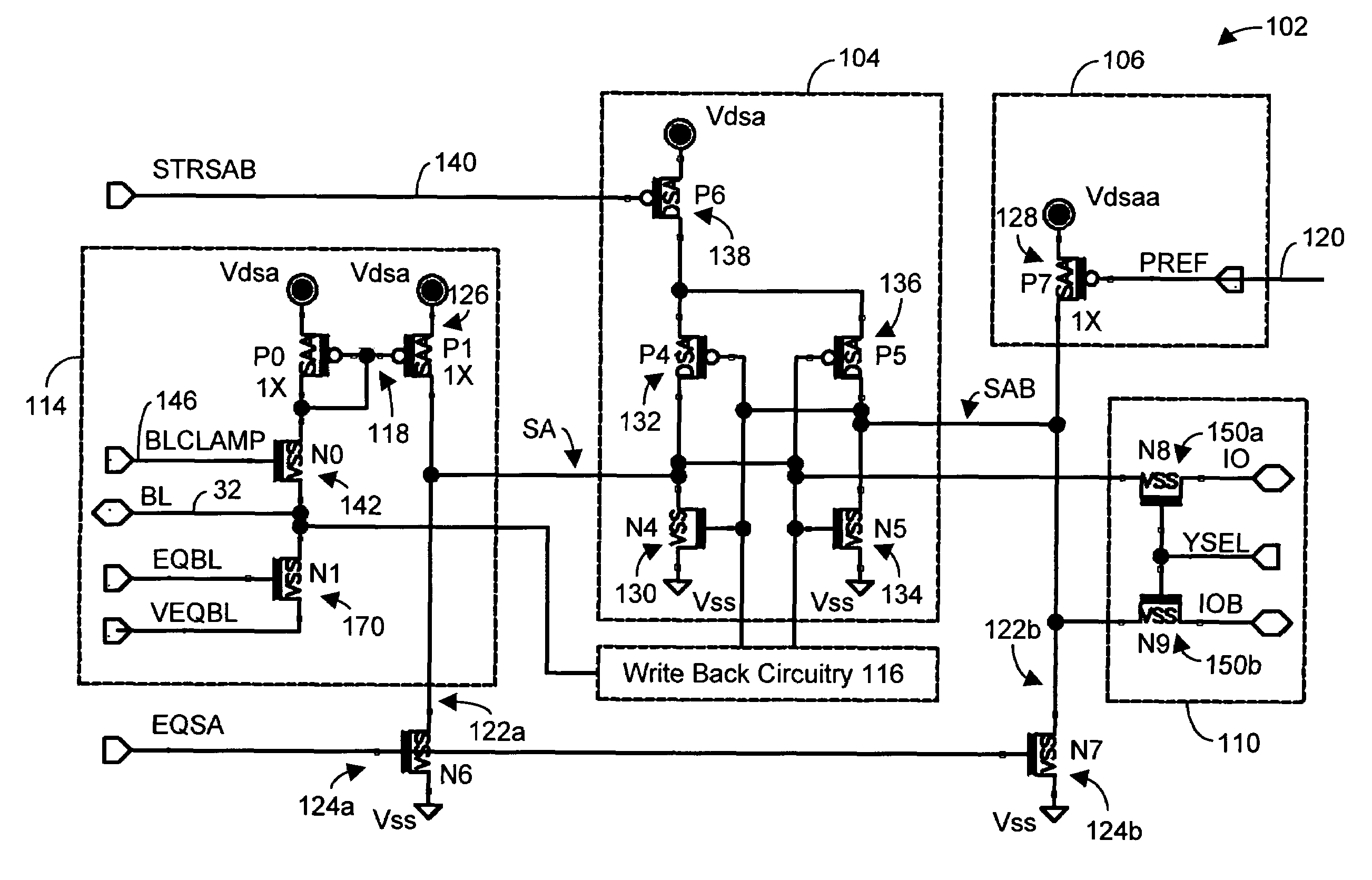
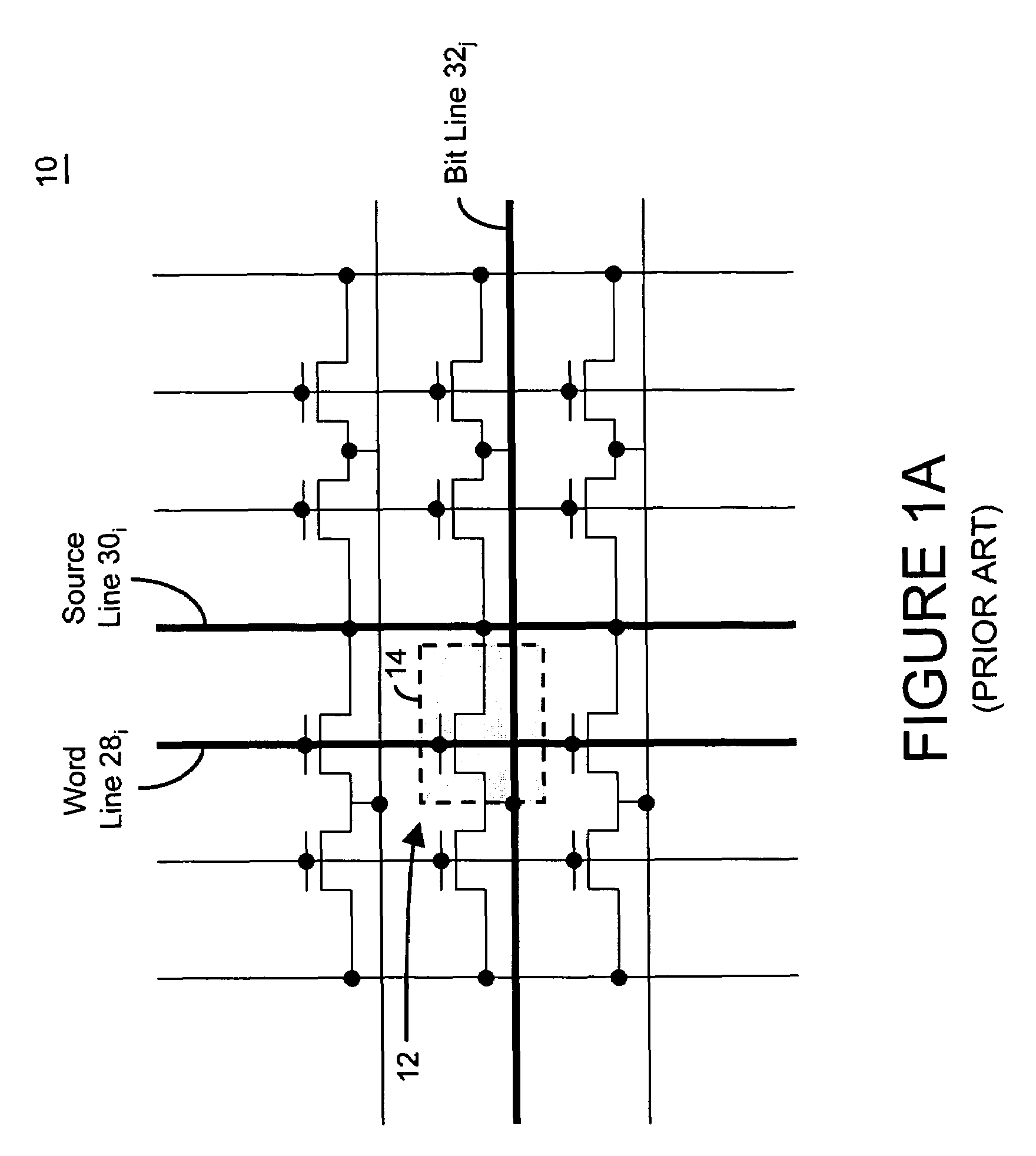
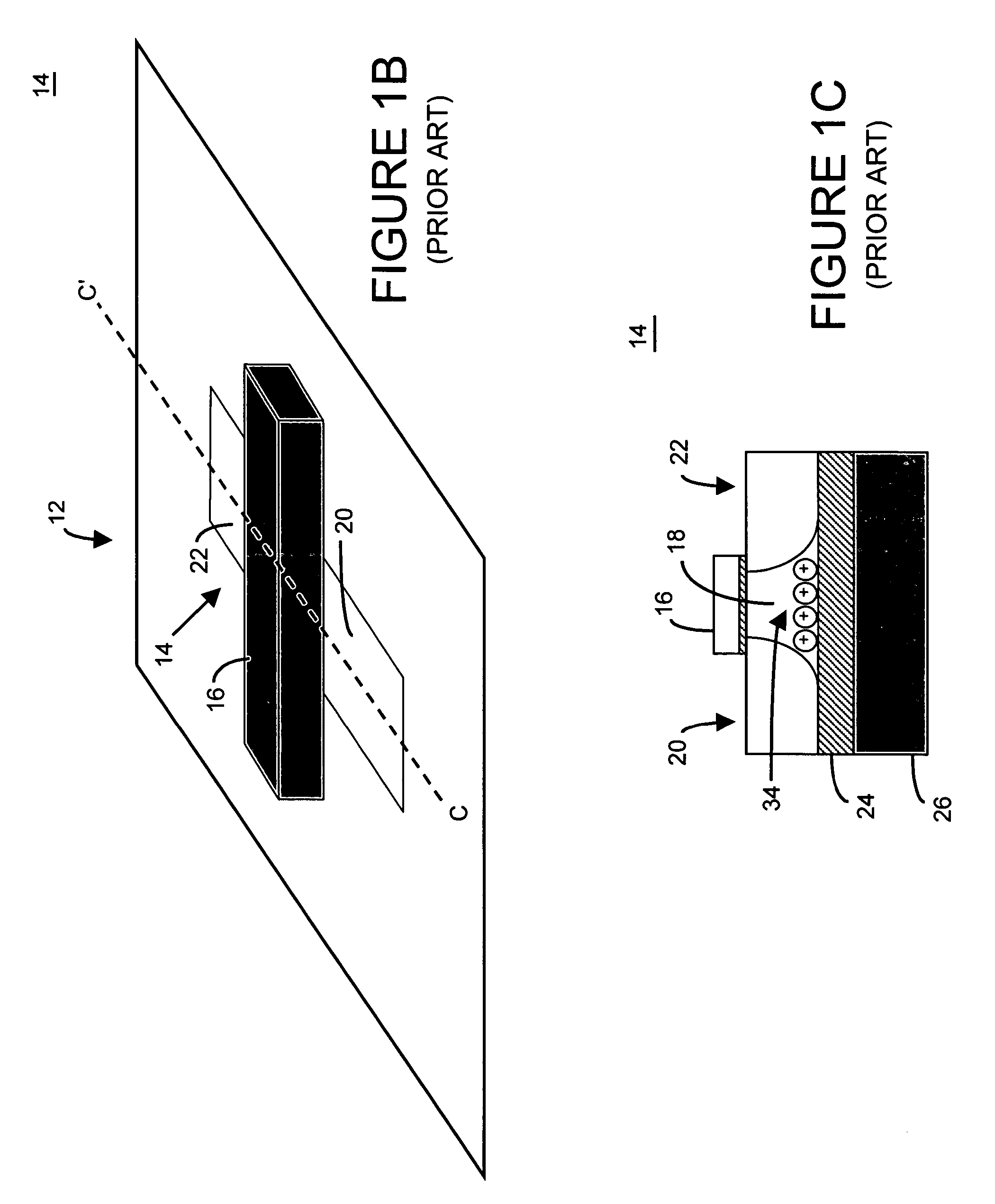
[0064]There are many inventions described and illustrated herein. In one aspect, the present inventions are directed to a technique of, and circuitry for sampling, sensing, reading and / or determining the data state of a memory cell of a memory cell array (for example, a memory cell array having a plurality of memory cells which consist of an electrically floating body transistor). In one embodiment, the present inventions include sense amplifier circuitry that is relatively compact and pitched to the array of memory cells such that a row of data may be read, sampled and / or sensed during a read operation. In this regard, an entire row of memory cells may be accessed and read during one operation which, relative to at least architecture employing multiplexer circuitry, may minimize, enhance and / or improve read latency and read access time, memory cell disturbance and / or simplify the control of the sense amplifier circuitry and access thereof.

[0065]In this embodiment, the sense amplifi...


PUM


Abstract

A technique of, and circuitry for sampling, sensing, reading and / or determining the data state of a memory cell of a memory cell array (for example, a memory cell array having a plurality of memory cells which consist of an electrically floating body transistor). In one embodiment, sense amplifier circuitry is relatively compact and pitched to the array of memory cells such that a row of data may be read, sampled and / or sensed during a read operation. In this regard, an entire row of memory cells may be accessed and read during one operation which, relative to at least architecture employing multiplexer circuitry, may minimize, enhance and / or improve read latency and read access time, memory cell disturbance and / or simplify the control of the sense amplifier circuitry and access thereof. The sense amplifier circuitry may include write back circuitry to modify or “re-store” the data read, sampled and / or sensed during a read operation and / or a refresh operation in the context of a DRAM array. The sense amplifier circuitry of this embodiment restores and / or refreshes data in an entire row of volatile and / or destructive read type memory cells in parallel. This architecture may minimize, enhance and / or improve write back and read latency parameters, relative to at least architecture employing multiplexer circuitry. Also, data that has been read, sampled and / or sensed by the sense amplifier circuitry during a read operation may be modified before being written back to one or more of the memory cells of the selected row of the array of memory cells.

Description

RELATED APPLICATIONS[0001]This application claims priority to U.S. Provisional Application Ser. No. 60 / 635,709, entitled “Sense Amplifier Circuitry and Architecture to Write Data Into and / or Read from Memory Cells”, filed Dec. 13, 2004. The contents of this provisional application are incorporated by reference herein in their entirety.BACKGROUND[0002]The inventions relate to semiconductor integrated circuit devices (for example, memory devices); and more particularly, in one aspect, to circuitry and techniques to write and read, sense and / or sample a data state to / from memory cells of a memory array and / or device, for example, a semiconductor dynamic random access memory (“DRAM”) device, wherein the memory cells have an electrically floating body in which an electrical charge is stored.[0003]There is a continuing trend to employ and / or fabricate advanced integrated circuits using techniques, materials and devices that improve performance, reduce leakage current and enhance overall s...

Claims


Application Information

Patent Timeline
Patent Type & Authority Patents(United States)
IPC IPC(8): G11C7/00
CPCG11C7/065G11C11/4091H01L29/7841H01L27/108H01L27/10802G11C7/14G11C11/4099G11C2211/4016G11C2211/4013H10B12/20H10B12/00
Inventor WALLER, WILLIAM KENNETHCARMAN, ERIC
Owner MICRON TECH INC
Learn More